Frontiers of Physics ( IF 6.5 ) Pub Date : 2024-04-04 , DOI: 10.1007/s11467-023-1390-3 Xueping Li , Xiaojie Tang , Zhuojun Wang , Peize Yuan , Lin Li , Chenhai Shen , Congxin Xia
|
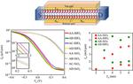
Dielectric engineering plays a crucial role in the process of device miniaturization. Herein we investigate the electrical properties of bilayer GaSe metal-oxide-semiconductor field-effect transistors (MOSFETs), considering hetero-gate-dielectric construction, dielectric materials and GaSe stacking pattern. The results show that device performance strongly depends on the dielectric constants and locations of insulators. When high-k dielectric is placed close to the drain, it behaves with a larger on-state current (Ion) of 5052 µA/µm when the channel is 5 nm. Additionally, when the channel is 5 nm and insulator is HfO2, the largest Ion is 5134 µA/µm for devices with AC stacking GaSe channel. In particular, when the gate length is 2 nm, it still meets the HP requirements of ITRS 2028 for the device with AA stacking when high-k dielectric is used. Hence, the work provides guidance to regulate the performance of the two-dimensional nanodevices by dielectric engineering.
中文翻译:
亚 5 nm 双层 GaSe MOSFET 实现超高通态电流
介电工程在器件小型化过程中起着至关重要的作用。在此,我们研究了双层 GaSe 金属氧化物半导体场效应晶体管 (MOSFET) 的电特性,考虑了异质栅极电介质结构、电介质材料和 GaSe 堆叠模式。结果表明,器件性能很大程度上取决于介电常数和绝缘体的位置。当高k电介质靠近漏极放置时,当沟道为 5 nm 时,它会表现出 5052 µA/µm 的较大通态电流 ( I on )。此外,当沟道为 5 nm、绝缘体为 HfO 2时,对于具有 AC 堆叠 GaSe 沟道的器件,最大 Ion 为 5134 µA / μm 。特别是,当栅极长度为2 nm时,在使用高k电介质时,仍然满足ITRS 2028对AA堆叠器件的HP要求。因此,这项工作为通过介电工程调节二维纳米器件的性能提供了指导。


 京公网安备 11010802027423号