npj Quantum Information ( IF 6.6 ) Pub Date : 2024-03-13 , DOI: 10.1038/s41534-024-00826-9 Davide Degli Esposti , Lucas E. A. Stehouwer , Önder Gül , Nodar Samkharadze , Corentin Déprez , Marcel Meyer , Ilja N. Meijer , Larysa Tryputen , Saurabh Karwal , Marc Botifoll , Jordi Arbiol , Sergey V. Amitonov , Lieven M. K. Vandersypen , Amir Sammak , Menno Veldhorst , Giordano Scappucci
|
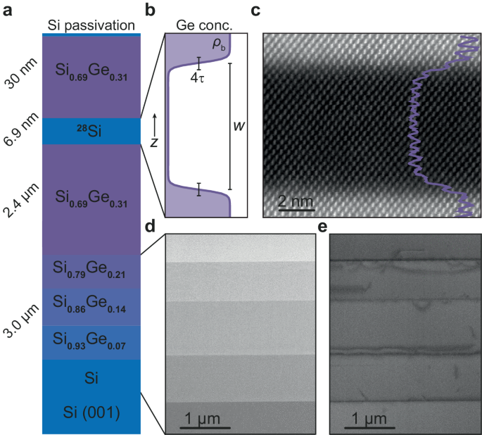
The electrical characterisation of classical and quantum devices is a critical step in the development cycle of heterogeneous material stacks for semiconductor spin qubits. In the case of silicon, properties such as disorder and energy separation of conduction band valleys are commonly investigated individually upon modifications in selected parameters of the material stack. However, this reductionist approach fails to consider the interdependence between different structural and electronic properties at the danger of optimising one metric at the expense of the others. Here, we achieve a significant improvement in both disorder and valley splitting by taking a co-design approach to the material stack. We demonstrate isotopically purified, strained quantum wells with high mobility of 3.14(8) × 105 cm2 V−1 s−1 and low percolation density of 6.9(1) × 1010 cm−2. These low disorder quantum wells support quantum dots with low charge noise of 0.9(3) μeV Hz−1/2 and large mean valley splitting energy of 0.24(7) meV, measured in qubit devices. By striking the delicate balance between disorder, charge noise, and valley splitting, these findings provide a benchmark for silicon as a host semiconductor for quantum dot qubits. We foresee the application of these heterostructures in larger, high-performance quantum processors.
中文翻译:
硅中的低无序度和高谷分裂
经典和量子器件的电学表征是半导体自旋量子位异质材料堆栈开发周期中的关键步骤。就硅而言,导带谷的无序性和能量分离等特性通常是在材料堆叠的选定参数修改后单独研究的。然而,这种还原论方法未能考虑不同结构和电子特性之间的相互依赖性,从而存在以牺牲其他指标为代价来优化一个指标的危险。在这里,我们通过对材料堆栈采取协同设计方法,在无序和谷分裂方面取得了显着改善。我们证明了同位素纯化的应变量子阱,具有 3.14(8) × 10 5 cm 2 V -1 s -1的高迁移率和 6.9(1) × 10 10 cm -2的低渗流密度。这些低无序量子阱支持具有 0.9(3) μeV Hz -1/2的低电荷噪声和 0.24(7) meV 的大平均谷分裂能(在量子位器件中测量)的量子点。通过在无序、电荷噪声和谷分裂之间取得微妙的平衡,这些发现为硅作为量子点量子位的主体半导体提供了基准。我们预见这些异质结构将在更大的高性能量子处理器中得到应用。


 京公网安备 11010802027423号