当前位置:
X-MOL 学术
›
Small Struct.
›
论文详情
Our official English website, www.x-mol.net, welcomes your
feedback! (Note: you will need to create a separate account there.)
Synthesis of NbSe2/Bilayer Nb-Doped WSe2 Heterostructure from Exfoliated WSe2 Flakes
Small Structures ( IF 13.9 ) Pub Date : 2024-02-12 , DOI: 10.1002/sstr.202300401 Van Tu Vu 1 , Minh Chien Nguyen 1 , Whan Kyun Kim 2, 3 , Van Dam Do 1 , Vu Khac Dat 4 , Woo Jong Yu 1
Small Structures ( IF 13.9 ) Pub Date : 2024-02-12 , DOI: 10.1002/sstr.202300401 Van Tu Vu 1 , Minh Chien Nguyen 1 , Whan Kyun Kim 2, 3 , Van Dam Do 1 , Vu Khac Dat 4 , Woo Jong Yu 1
Affiliation
|
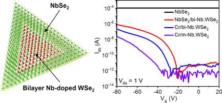
Forming heterostructures of 2D metals and semiconductors using chemical vapor deposition (CVD) has significant potential to effectively reduce contact resistance in electronic devices. However, semiconducting transition metal dichalcogenide (TMD) layers in metal–semiconductor heterostructures are currently restricted to monolayers despite the superior mobility and density of states in bilayer TMDs. Herein, NbSe2/bilayer Nb-doped WSe2 metal/semiconductor heterostructure from exfoliated WSe2 flakes are synthesized first. The exfoliated WSe2 bulk crystals on an Nb-coated substrate are heated to 950 °C under a flow of selenium vapor, and then the NbSe2/bilayer Nb-doped WSe2 heterostructures are formed. Statistics on the number of Nb-doped WSe2 layers grown on a 1 cm × 1 cm CVD substrate shows that 65% of the Nb-doped WSe2 layers are grown as bilayers. X-ray photoelectron spectroscopy, optical microscopy, and transmission electron microscopy clearly clarify the number of Nb-doped WSe2 layers and heterostructure of NbSe2/bilayer Nb-doped WSe2. Electrical measurements using Cr contacts show that bilayer Nb-doped WSe2 displays 7- and 10-times higher mobility and on/off ratio than monolayer Nb-doped WSe2. The mobility and on/off ratio are further doubled in NbSe2/bilayer Nb-doped WSe2 contact compared to Cr/bilayer Nb-doped WSe2 contact, attributed to a clean interface in vertical stack heterostructure, enhancing electrical performance.
中文翻译:

利用剥离的 WSe2 薄片合成 NbSe2/双层 Nb 掺杂 WSe2 异质结构
使用化学气相沉积 (CVD) 形成二维金属和半导体异质结构具有有效降低电子设备接触电阻的巨大潜力。然而,尽管双层TMD具有优异的迁移率和态密度,但金属-半导体异质结构中的半导体过渡金属二硫属化物(TMD)层目前仅限于单层。在此,首先从剥离的WSe 2薄片合成NbSe 2 /双层Nb掺杂的WSe 2金属/半导体异质结构。在硒蒸气流下将Nb涂覆基底上剥离的WSe 2块状晶体加热至950℃,然后形成NbSe 2 /双层Nb掺杂WSe 2异质结构。对在 1 cm × 1 cm CVD 衬底上生长的 Nb 掺杂 WSe 2层数量的统计表明,65%的 Nb 掺杂 WSe 2层生长为双层。 X射线光电子能谱、光学显微镜和透射电子显微镜清楚地阐明了Nb掺杂WSe 2的层数和NbSe 2 /双层Nb掺杂WSe 2的异质结构。使用 Cr 接触的电学测量表明,双层 Nb 掺杂 WSe 2的迁移率和开/关比比单层 Nb 掺杂 WSe 2高 7 倍和 10 倍。与Cr/双层Nb掺杂WSe 2接触相比, NbSe 2 /双层Nb掺杂WSe 2接触的迁移率和开/关比进一步加倍,这归因于垂直堆叠异质结构中的干净界面,从而增强了电性能。
更新日期:2024-02-12
中文翻译:
利用剥离的 WSe2 薄片合成 NbSe2/双层 Nb 掺杂 WSe2 异质结构
使用化学气相沉积 (CVD) 形成二维金属和半导体异质结构具有有效降低电子设备接触电阻的巨大潜力。然而,尽管双层TMD具有优异的迁移率和态密度,但金属-半导体异质结构中的半导体过渡金属二硫属化物(TMD)层目前仅限于单层。在此,首先从剥离的WSe 2薄片合成NbSe 2 /双层Nb掺杂的WSe 2金属/半导体异质结构。在硒蒸气流下将Nb涂覆基底上剥离的WSe 2块状晶体加热至950℃,然后形成NbSe 2 /双层Nb掺杂WSe 2异质结构。对在 1 cm × 1 cm CVD 衬底上生长的 Nb 掺杂 WSe 2层数量的统计表明,65%的 Nb 掺杂 WSe 2层生长为双层。 X射线光电子能谱、光学显微镜和透射电子显微镜清楚地阐明了Nb掺杂WSe 2的层数和NbSe 2 /双层Nb掺杂WSe 2的异质结构。使用 Cr 接触的电学测量表明,双层 Nb 掺杂 WSe 2的迁移率和开/关比比单层 Nb 掺杂 WSe 2高 7 倍和 10 倍。与Cr/双层Nb掺杂WSe 2接触相比, NbSe 2 /双层Nb掺杂WSe 2接触的迁移率和开/关比进一步加倍,这归因于垂直堆叠异质结构中的干净界面,从而增强了电性能。


 京公网安备 11010802027423号