当前位置:
X-MOL 学术
›
J. Phys. Chem. C
›
论文详情
Our official English website, www.x-mol.net, welcomes your
feedback! (Note: you will need to create a separate account there.)
Tuning the Electronic and Photoelectronic Properties of Two-Dimensional MoSe2 Thin Films by In Situ V-Doping
The Journal of Physical Chemistry C ( IF 3.3 ) Pub Date : 2024-01-11 , DOI: 10.1021/acs.jpcc.3c06829
Caimei Li 1 , Yutong Wang 1 , Heng Yang 2 , Wen-Jie Wang 1 , Fangchao Lu 1 , Xiaolong Liu 2 , Xun-Lei Ding 1, 3 , Jiajun Deng 1
The Journal of Physical Chemistry C ( IF 3.3 ) Pub Date : 2024-01-11 , DOI: 10.1021/acs.jpcc.3c06829
Caimei Li 1 , Yutong Wang 1 , Heng Yang 2 , Wen-Jie Wang 1 , Fangchao Lu 1 , Xiaolong Liu 2 , Xun-Lei Ding 1, 3 , Jiajun Deng 1
Affiliation
|
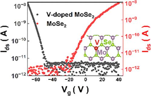
Atom-substituting doping by atmospheric-pressure chemical vapor deposition (AP-CVD) is an effective and promising strategy for changing the properties of two-dimensional transition-metal dichalcogenides (2D TMDs). In this paper, we successfully grew V-doped MoSe2 films. The photoluminescence (PL) spectra gradually red-shifted with the increase of the doping concentration, the X-ray photoelectron spectroscopy (XPS) after doping shifted toward a lower binding energy, and the change of polarity before and after doping can be seen in the transfer characteristic curves of back-gated field-effect transistors (FETs) based on V-doped and undoped MoSe2 films and proves that the V atom successfully replaces the Mo atom and acts as a p-type dopant, which greatly improves the properties of back-gated FETs based on 2D V-doped MoSe2. The hole mobility of the doped samples can reach 111.34 cm2 V–1 s–1, the Ion/Ioff ratio of the hole branch can reach 107, and the detector has a fast response time of 2.3 ms. The results show that the band gap, polarity, optical properties, and electrical properties of 2D MoSe2 can be effectively adjusted by changing the V concentration, which provide a feasible way for 2D materials to realize high-performance scalable microelectronic devices and also provide new opportunities for 2D materials in electronic or optoelectronic applications.
中文翻译:

通过原位 V 掺杂调节二维 MoSe2 薄膜的电子和光电性能
通过大气压化学气相沉积(AP-CVD)进行原子取代掺杂是改变二维过渡金属二硫属化物(2D TMD)性能的有效且有前途的策略。在本文中,我们成功生长了V掺杂的MoSe 2薄膜。随着掺杂浓度的增加,光致发光(PL)光谱逐渐红移,掺杂后的X射线光电子能谱(XPS)向较低结合能方向移动,掺杂前后极性发生变化。基于V掺杂和未掺杂MoSe 2薄膜的背栅场效应晶体管(FET)的传输特性曲线,证明V原子成功取代Mo原子并充当p型掺杂剂,极大地提高了器件的性能基于 2D V 掺杂 MoSe 2的背栅 FET 。掺杂样品的空穴迁移率可达111.34 cm 2 V –1 s –1,空穴分支的I on / I off比可达10 7,探测器具有2.3 ms的快速响应时间。研究结果表明,通过改变V浓度可以有效调节二维MoSe 2的带隙、极性、光学性质和电学性质,为二维材料实现高性能可扩展微电子器件提供了可行途径,也为二维材料提供了新的可扩展微电子器件。二维材料在电子或光电应用中的机会。
更新日期:2024-01-11
中文翻译:
通过原位 V 掺杂调节二维 MoSe2 薄膜的电子和光电性能
通过大气压化学气相沉积(AP-CVD)进行原子取代掺杂是改变二维过渡金属二硫属化物(2D TMD)性能的有效且有前途的策略。在本文中,我们成功生长了V掺杂的MoSe 2薄膜。随着掺杂浓度的增加,光致发光(PL)光谱逐渐红移,掺杂后的X射线光电子能谱(XPS)向较低结合能方向移动,掺杂前后极性发生变化。基于V掺杂和未掺杂MoSe 2薄膜的背栅场效应晶体管(FET)的传输特性曲线,证明V原子成功取代Mo原子并充当p型掺杂剂,极大地提高了器件的性能基于 2D V 掺杂 MoSe 2的背栅 FET 。掺杂样品的空穴迁移率可达111.34 cm 2 V –1 s –1,空穴分支的I on / I off比可达10 7,探测器具有2.3 ms的快速响应时间。研究结果表明,通过改变V浓度可以有效调节二维MoSe 2的带隙、极性、光学性质和电学性质,为二维材料实现高性能可扩展微电子器件提供了可行途径,也为二维材料提供了新的可扩展微电子器件。二维材料在电子或光电应用中的机会。


 京公网安备 11010802027423号