当前位置:
X-MOL 学术
›
Cryst. Growth Des.
›
论文详情
Our official English website, www.x-mol.net, welcomes your
feedback! (Note: you will need to create a separate account there.)
Synthesis and Characterization of a Porous Ga2O3 Material with a Low Dielectric Constant
Crystal Growth & Design ( IF 3.2 ) Pub Date : 2023-12-26 , DOI: 10.1021/acs.cgd.3c01233
Xue Dong 1 , Chaeheon Woo 2 , Chan-Sei Yoo 3 , Tae Yeong Kim 2 , Xiaojie Zhang 2 , Yeongjin Kim 2 , Jinsu Kang 2 , Jiho Jeon 2, 4, 5 , Hyeon-Seok Bang 2, 4, 5 , Youngho Kim 6, 7 , Jae-Hyuk Park 2 , Hak Ki Yu 6 , Jae-Young Choi 1, 2, 4
Affiliation
|
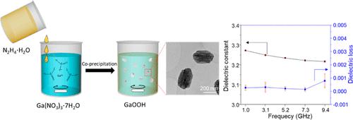
In the context of contemporary wireless communication technologies, operational frequencies have considerably escalated. Consequently, the demand for dielectric ceramics with low dielectric constants and minimal losses has become imperative in the field. Thermally stable β-Ga2O3 was synthesized by a simple chemical precipitation route followed by calcination, making it a promising candidate for microwave applications. The as-prepared β-Ga2O3 maintained a pore structure with a width of 20.943 nm. Notably, the material exhibited early-stage sintering at relatively low temperatures, around 900 °C, due to these pores. The as-prepared β-Ga2O3 ceramics exhibited outstanding dielectric properties, featuring a lower εr value of 3.2168 and a low dielectric loss of 0.000795 at 9.4 GHz. The lower εr contributes to minimized time delays, while the low dielectric loss enhances the signal selectivity. These findings establish β-Ga2O3 as a suitable material for electronic packaging in microwave applications.
中文翻译:

低介电常数Ga2O3多孔材料的合成与表征
在当代无线通信技术的背景下,工作频率已大大提高。因此,该领域迫切需要具有低介电常数和最小损耗的介电陶瓷。热稳定的β-Ga 2 O 3通过简单的化学沉淀路线和煅烧合成,使其成为微波应用的有希望的候选者。所制备的β-Ga 2 O 3保持宽度为20.943 nm的孔结构。值得注意的是,由于这些孔隙,该材料在相对较低的温度(约 900°C)下表现出早期烧结。所制备的β-Ga 2 O 3陶瓷表现出优异的介电性能,在9.4 GHz时具有较低的ε r值(3.2168)和低介电损耗(0.000795)。较低的 ε r有助于最小化时间延迟,而低介电损耗则增强了信号选择性。这些发现表明 β-Ga 2 O 3是微波应用中电子封装的合适材料。
更新日期:2023-12-26
中文翻译:
低介电常数Ga2O3多孔材料的合成与表征
在当代无线通信技术的背景下,工作频率已大大提高。因此,该领域迫切需要具有低介电常数和最小损耗的介电陶瓷。热稳定的β-Ga 2 O 3通过简单的化学沉淀路线和煅烧合成,使其成为微波应用的有希望的候选者。所制备的β-Ga 2 O 3保持宽度为20.943 nm的孔结构。值得注意的是,由于这些孔隙,该材料在相对较低的温度(约 900°C)下表现出早期烧结。所制备的β-Ga 2 O 3陶瓷表现出优异的介电性能,在9.4 GHz时具有较低的ε r值(3.2168)和低介电损耗(0.000795)。较低的 ε r有助于最小化时间延迟,而低介电损耗则增强了信号选择性。这些发现表明 β-Ga 2 O 3是微波应用中电子封装的合适材料。


 京公网安备 11010802027423号