当前位置:
X-MOL 学术
›
Adv. Funct. Mater.
›
论文详情
Our official English website, www.x-mol.net, welcomes your
feedback! (Note: you will need to create a separate account there.)
Highly Selective Nano-Interface Engineering in Multishelled Nanocubes for Enhanced Broadband Electromagnetic Attenuation
Advanced Functional Materials ( IF 18.5 ) Pub Date : 2023-12-27 , DOI: 10.1002/adfm.202313829 Huibin Zhang 1, 2 , Xiaodi Zhou 2 , Mingyue Yuan 2 , Xuhui Xiong 1 , Xiaowei Lv 2 , Yihao Liu 2 , Hualiang Lv 3 , Yuxiang Lai 4 , Jincang Zhang 5 , Huiran Zhang 1 , Deng Pan 1 , Renchao Che 2, 5
Advanced Functional Materials ( IF 18.5 ) Pub Date : 2023-12-27 , DOI: 10.1002/adfm.202313829 Huibin Zhang 1, 2 , Xiaodi Zhou 2 , Mingyue Yuan 2 , Xuhui Xiong 1 , Xiaowei Lv 2 , Yihao Liu 2 , Hualiang Lv 3 , Yuxiang Lai 4 , Jincang Zhang 5 , Huiran Zhang 1 , Deng Pan 1 , Renchao Che 2, 5
Affiliation
|
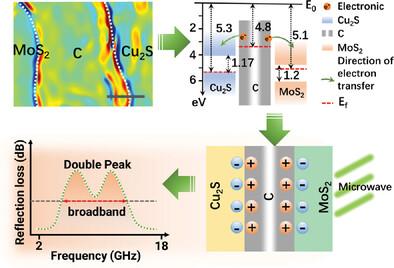
Within the nanoscale, methodically reconfiguring interface charges, and leveraging this newly structured interface to modify the energy-momentum dynamics of heterojunction energy bands, hold profound implications for microwave electronics because of the intensified interaction between external microwaves and interfaces of materials. Mastering the orderly reconstruction of interface charges, contingent upon precise control over composition, orientation, and electronic structure remains a challenge at this scale. Herein, an in situ hierarchical assembly approach is used to successively deposit layers of Cu2S, C, and MoS2 on a hollow cubic framework with a thickness of 20 nm. Additionally, by harnessing the quasi-graphitic characteristics and elevated work function of graphitized carbon in the middle layer, its inherent charge is steered toward both the outer and inner layers, establishing a structured configuration for the crafted Cu2S@C and C@MoS2 interfaces. Employing advanced off-axis electron holography, microwave dielectric measurements, and first-principle calculations, the dynamic reconstruction of interface charges and the resulting microwave response is ascertained. The synergistic effect revealed that the Cu2S@C@MoS2 materials exhibited exceptional microwave absorption, with an effective absorption band covering 7.03 GHz at 2.0 mm thickness. Furthermore, the orderly reconstruction of nano-interfaces paves the way for research into novel electromagnetic protection materials and their unique electronic behaviors.
中文翻译:

多壳纳米立方体中的高选择性纳米界面工程可增强宽带电磁衰减
在纳米尺度内,有条不紊地重新配置界面电荷,并利用这种新结构的界面来改变异质结能带的能量动量动力学,对微波电子学具有深远的影响,因为外部微波与材料界面之间的相互作用增强。掌握界面电荷的有序重建,取决于对成分、方向和电子结构的精确控制,在这种规模上仍然是一个挑战。在此,采用原位分层组装方法在厚度为20 nm的空心立方框架上连续沉积Cu 2 S、C和MoS 2层。此外,通过利用中间层石墨化碳的准石墨特性和升高的功函数,其固有电荷被引导至外层和内层,从而为精心制作的 Cu 2 S@C 和 C@MoS建立了结构化配置2个接口。采用先进的离轴电子全息术、微波介电测量和第一原理计算,确定了界面电荷的动态重建和由此产生的微波响应。协同效应表明,Cu 2 S@C@MoS 2材料表现出优异的微波吸收能力,在2.0 mm厚度下有效吸收带覆盖7.03 GHz。此外,纳米界面的有序重构为研究新型电磁防护材料及其独特的电子行为铺平了道路。
更新日期:2023-12-27
中文翻译:
多壳纳米立方体中的高选择性纳米界面工程可增强宽带电磁衰减
在纳米尺度内,有条不紊地重新配置界面电荷,并利用这种新结构的界面来改变异质结能带的能量动量动力学,对微波电子学具有深远的影响,因为外部微波与材料界面之间的相互作用增强。掌握界面电荷的有序重建,取决于对成分、方向和电子结构的精确控制,在这种规模上仍然是一个挑战。在此,采用原位分层组装方法在厚度为20 nm的空心立方框架上连续沉积Cu 2 S、C和MoS 2层。此外,通过利用中间层石墨化碳的准石墨特性和升高的功函数,其固有电荷被引导至外层和内层,从而为精心制作的 Cu 2 S@C 和 C@MoS建立了结构化配置2个接口。采用先进的离轴电子全息术、微波介电测量和第一原理计算,确定了界面电荷的动态重建和由此产生的微波响应。协同效应表明,Cu 2 S@C@MoS 2材料表现出优异的微波吸收能力,在2.0 mm厚度下有效吸收带覆盖7.03 GHz。此外,纳米界面的有序重构为研究新型电磁防护材料及其独特的电子行为铺平了道路。


 京公网安备 11010802027423号