当前位置:
X-MOL 学术
›
Adv. Opt. Mater.
›
论文详情
Our official English website, www.x-mol.net, welcomes your feedback! (Note: you will need to create a separate account there.)
Single Photon Emitters in Hexagonal Boron Nitride Fabricated by Focused Helium Ion Beam
Advanced Optical Materials ( IF 8.0 ) Pub Date : 2023-11-27 , DOI: 10.1002/adom.202302083 Guan‐Lin Liu 1, 2 , Xin‐Yu Wu 1, 2 , Peng‐Tao Jing 1 , Zhen Cheng 1 , Da Zhan 1 , Yang Bao 1 , Jia‐Xu Yan 1 , Hai Xu 1 , Li‐Gong Zhang 1 , Bing‐Hui Li 1 , Ke‐Wei Liu 1 , Lei Liu 1 , De‐Zhen Shen 1
Advanced Optical Materials ( IF 8.0 ) Pub Date : 2023-11-27 , DOI: 10.1002/adom.202302083 Guan‐Lin Liu 1, 2 , Xin‐Yu Wu 1, 2 , Peng‐Tao Jing 1 , Zhen Cheng 1 , Da Zhan 1 , Yang Bao 1 , Jia‐Xu Yan 1 , Hai Xu 1 , Li‐Gong Zhang 1 , Bing‐Hui Li 1 , Ke‐Wei Liu 1 , Lei Liu 1 , De‐Zhen Shen 1
Affiliation
|
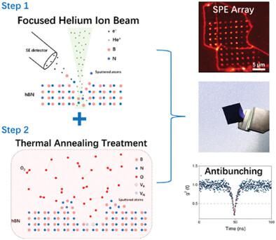
The 2D layered hexagonal boron nitride (hBN) material is a promising platform for making single photon emitters (SPEs). Integrate SPEs with photonic cavities or waveguides, requires the deterministic positioning of these emitters as accurately as possible. Among all of the alternative techniques, He+ focused ion beam (FIB) theoretically has sub-nanometer precision, but its practical positioning accuracy in processing SPEs is limited by the inevitable detrimental byproduct defects. So far, it remains challenging to achieve an accuracy below 100 nm for the positioning of SPEs in hBN. Here, we present a two-step method for creating SPEs at the predetermined positions in hBN that combines the He+ FIB irradiation and thermal annealing under an oxygen atmosphere. With this method, we have realized the positioning accuracy of less than 50 nm, which, to the best of our knowledge, stands as the highest among the currently available hBN SPEs preparation methods. Moreover, the SPE conversion yield was over 35% and the emission brightness of individual SPE achieved up to 3 × 10⁵ counts/s at room temperature. These SPEs fabricated precisely with nanoscale accuracy in hBN are expected to be good candidates for making large-scale integrated SPEs in photonic circuits.
中文翻译:

聚焦氦离子束制备的六方氮化硼单光子发射器
二维层状六方氮化硼(hBN)材料是制造单光子发射器(SPE)的有前途的平台。将 SPE 与光子腔或波导集成,需要尽可能准确地确定这些发射器的定位。在所有替代技术中,He +聚焦离子束 (FIB) 理论上具有亚纳米精度,但其在处理 SPE 时的实际定位精度受到不可避免的有害副产品缺陷的限制。到目前为止,在 hBN 中实现 SPE 定位精度低于 100 nm 仍然具有挑战性。在这里,我们提出了一种在 hBN 中预定位置创建 SPE 的两步方法,该方法结合了 He + FIB 辐射和氧气气氛下的热退火。通过该方法,我们实现了小于50 nm的定位精度,据我们所知,这是目前可用的hBN SPE制备方法中最高的。此外,SPE转化率超过35%,室温下单个SPE的发射亮度达到3×10 5 counts/s。这些在 hBN 中以纳米级精度精确制造的 SPE 有望成为在光子电路中制造大规模集成 SPE 的良好候选者。
更新日期:2023-11-27
中文翻译:
聚焦氦离子束制备的六方氮化硼单光子发射器
二维层状六方氮化硼(hBN)材料是制造单光子发射器(SPE)的有前途的平台。将 SPE 与光子腔或波导集成,需要尽可能准确地确定这些发射器的定位。在所有替代技术中,He +聚焦离子束 (FIB) 理论上具有亚纳米精度,但其在处理 SPE 时的实际定位精度受到不可避免的有害副产品缺陷的限制。到目前为止,在 hBN 中实现 SPE 定位精度低于 100 nm 仍然具有挑战性。在这里,我们提出了一种在 hBN 中预定位置创建 SPE 的两步方法,该方法结合了 He + FIB 辐射和氧气气氛下的热退火。通过该方法,我们实现了小于50 nm的定位精度,据我们所知,这是目前可用的hBN SPE制备方法中最高的。此外,SPE转化率超过35%,室温下单个SPE的发射亮度达到3×10 5 counts/s。这些在 hBN 中以纳米级精度精确制造的 SPE 有望成为在光子电路中制造大规模集成 SPE 的良好候选者。


 京公网安备 11010802027423号