Journal of Alloys and Compounds ( IF 5.8 ) Pub Date : 2023-11-28 , DOI: 10.1016/j.jallcom.2023.172946
Yiming Shi , Junhua Meng , Jingren Chen , Rui Wu , Lisheng Zhang , Ji Jiang , Jinxiang Deng , Zhigang Yin , Xingwang Zhang
|
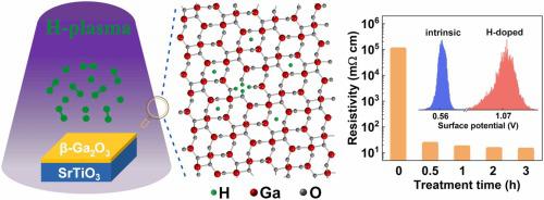
As a common impurity, H plays a role in tuning the electrical properties of β-Ga2O3 and has attracted immense interest. Despite years of investigations, the influence of H-doping on electrical properties is not always clear due to the lack of comprehensive characterization on both micro- and macro scale. In this work, we investigate the effects of the H-plasma treatment on the electrical properties of β-Ga2O3 films by combining several techniques, from macroscale Hall and photoluminescence measurements to microscale conductive atomic force microscopy (CAFM) and Kelvin probe force microscopy (KPFM). The incorporation of H in β-Ga2O3 not only introduces shallow donor states such as Hi, but also passivates VGa defects by forming the VGa-4H complex. As a result, both the carrier concentration and mobility of H-doped β-Ga2O3 film are significantly increased, corresponding to an enhancement of conductivity by four orders of magnitude in comparison with the intrinsic one. These results correlate well with the local conductivity and surface potential mappings obtained from CAFM and KPFM. Moreover, we found that the work function of β-Ga2O3 thin films can also be tuned by the H-plasma treatment.
中文翻译:
氢等离子体处理增强 β-Ga2O3 薄膜的电导率并降低功函数
作为一种常见的杂质,H在调节β-Ga 2 O 3的电性能方面发挥着重要作用,引起了人们的极大兴趣。尽管经过多年的研究,由于缺乏微观和宏观尺度的全面表征,氢掺杂对电性能的影响并不总是清楚。在这项工作中,我们通过结合多种技术,从宏观霍尔和光致发光测量到微观尺度传导原子力显微镜 (CAFM) 和开尔文探针力,研究 H 等离子体处理对 β-Ga 2 O 3薄膜电性能的影响显微镜(KPFM)。H在β-Ga 2 O 3中的掺入不仅引入了浅施主态例如H i,而且通过形成V Ga -4H络合物钝化了V Ga缺陷。结果,H掺杂β-Ga 2 O 3薄膜的载流子浓度和迁移率均显着增加,电导率比本征薄膜提高了四个数量级。这些结果与从 CAFM 和 KPFM 获得的局部电导率和表面电势映射很好地相关。此外,我们发现β-Ga 2 O 3薄膜的功函数也可以通过H等离子体处理来调节。


 京公网安备 11010802027423号