当前位置:
X-MOL 学术
›
Adv. Mater.
›
论文详情
Our official English website, www.x-mol.net, welcomes your
feedback! (Note: you will need to create a separate account there.)
Grain Engineering of Sb2S3 Thin Films to Enable Efficient Planar Solar Cells with High Open-Circuit Voltage
Advanced Materials ( IF 27.4 ) Pub Date : 2023-11-10 , DOI: 10.1002/adma.202305841
Xinnian Liu 1 , Zhiyuan Cai 2 , Lei Wan 1 , Peng Xiao 2 , Bo Che 2 , Junjie Yang 2 , Haihong Niu 1 , Huan Wang 1 , Jun Zhu 3 , Yi-Teng Huang 4 , Huimin Zhu 4, 5 , Szymon J Zelewski 6 , Tao Chen 2 , Robert L Z Hoye 4 , Ru Zhou 1, 4
Affiliation
|
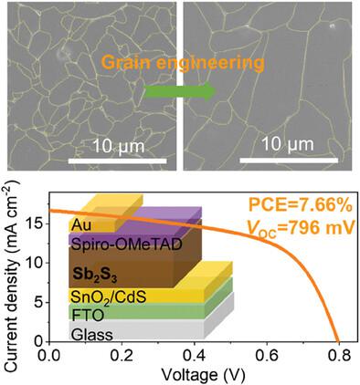
Sb2S3 is a promising environmentally friendly semiconductor for high performance solar cells. But, like many other polycrystalline materials, Sb2S3 is limited by nonradiative recombination and carrier scattering by grain boundaries (GBs). This work shows how the GB density in Sb2S3 films can be significantly reduced from 1068 ± 40 to 327 ± 23 nm µm−2 by incorporating an appropriate amount of Ce3+ into the precursor solution for Sb2S3 deposition. Through extensive characterization of structural, morphological, and optoelectronic properties, complemented with computations, it is revealed that a critical factor is the formation of an ultrathin Ce2S3 layer at the CdS/Sb2S3 interface, which can reduce the interfacial energy and increase the adhesion work between Sb2S3 and the substrate to encourage heterogeneous nucleation of Sb2S3, as well as promote lateral grain growth. Through reductions in nonradiative recombination at GBs and/or the CdS/Sb2S3 heterointerface, as well as improved charge-carrier transport properties at the heterojunction, this work achieves high performance Sb2S3 solar cells with a power conversion efficiency reaching 7.66%. An impressive open-circuit voltage (VOC) of 796 mV is achieved, which is the highest reported thus far for Sb2S3 solar cells. This work provides a strategy to simultaneously regulate the nucleation and growth of Sb2S3 absorber films for enhanced device performance.
中文翻译:

Sb2S3 薄膜的晶粒工程可实现具有高开路电压的高效平面太阳能电池
Sb 2 S 3是一种有前途的用于高性能太阳能电池的环保半导体。但是,与许多其他多晶材料一样,Sb 2 S 3受到非辐射复合和晶界 (GB) 载流子散射的限制。这项工作展示了如何通过将适量的Ce 3+掺入用于Sb 2 S 3沉积的前体溶液中,将Sb 2 S 3薄膜中的GB密度从1068 ± 40显着降低至327 ± 23 nm µm -2 。通过对结构、形态和光电性质的广泛表征,并辅以计算,揭示了一个关键因素是在CdS/Sb 2 S 3界面处形成超薄Ce 2 S 3层,这可以降低界面能增加Sb 2 S 3与基底之间的粘附功,以促进Sb 2 S 3的异质成核,并促进横向晶粒生长。通过减少GBs和/或CdS/Sb 2 S 3异质界面处的非辐射复合,以及改善异质结处的载流子传输特性,这项工作实现了高性能Sb 2 S 3太阳能电池,功率转换效率达到7.66 %。达到了令人印象深刻的 796 mV 开路电压 ( V OC ),这是迄今为止 Sb 2 S 3太阳能电池报道的最高电压。 这项工作提供了一种同时调节Sb 2 S 3吸收膜的成核和生长以增强器件性能的策略。
更新日期:2023-11-10
中文翻译:
Sb2S3 薄膜的晶粒工程可实现具有高开路电压的高效平面太阳能电池
Sb 2 S 3是一种有前途的用于高性能太阳能电池的环保半导体。但是,与许多其他多晶材料一样,Sb 2 S 3受到非辐射复合和晶界 (GB) 载流子散射的限制。这项工作展示了如何通过将适量的Ce 3+掺入用于Sb 2 S 3沉积的前体溶液中,将Sb 2 S 3薄膜中的GB密度从1068 ± 40显着降低至327 ± 23 nm µm -2 。通过对结构、形态和光电性质的广泛表征,并辅以计算,揭示了一个关键因素是在CdS/Sb 2 S 3界面处形成超薄Ce 2 S 3层,这可以降低界面能增加Sb 2 S 3与基底之间的粘附功,以促进Sb 2 S 3的异质成核,并促进横向晶粒生长。通过减少GBs和/或CdS/Sb 2 S 3异质界面处的非辐射复合,以及改善异质结处的载流子传输特性,这项工作实现了高性能Sb 2 S 3太阳能电池,功率转换效率达到7.66 %。达到了令人印象深刻的 796 mV 开路电压 ( V OC ),这是迄今为止 Sb 2 S 3太阳能电池报道的最高电压。 这项工作提供了一种同时调节Sb 2 S 3吸收膜的成核和生长以增强器件性能的策略。


 京公网安备 11010802027423号