Our official English website, www.x-mol.net, welcomes your
feedback! (Note: you will need to create a separate account there.)
Alternating BiI3–BiI van der Waals Photodetector with Low Dark Current and High-Performance Photodetection
ACS Nano ( IF 15.8 ) Pub Date : 2023-10-20 , DOI: 10.1021/acsnano.3c05849
Haoran Mu 1 , Renzhong Zhuang 2 , Nan Cui 1 , Songhua Cai 3 , Wenzhi Yu 1 , Jian Yuan 4 , Jingni Zhang 1 , Hao Liu 1 , Luyao Mei 1 , Xiaoyue He 1 , Zengxia Mei 1 , Guangyu Zhang 1, 5 , Qiaoliang Bao 6 , Shenghuang Lin 1
ACS Nano ( IF 15.8 ) Pub Date : 2023-10-20 , DOI: 10.1021/acsnano.3c05849
Haoran Mu 1 , Renzhong Zhuang 2 , Nan Cui 1 , Songhua Cai 3 , Wenzhi Yu 1 , Jian Yuan 4 , Jingni Zhang 1 , Hao Liu 1 , Luyao Mei 1 , Xiaoyue He 1 , Zengxia Mei 1 , Guangyu Zhang 1, 5 , Qiaoliang Bao 6 , Shenghuang Lin 1
Affiliation
|
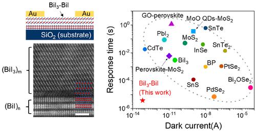
The emerging two-dimensional (2D) van der Waals (vdW) materials and their heterostructures hold great promise for optoelectronics and photonic applications beyond strictly lattice-matching constraints and grade interfaces. However, previous photodetectors and optoelectronic devices rely on relatively simple vdW heterostructures with one or two blocks. The realization of high-order heterostructures has been exponentially challenging due to conventional layer-by-layer arduous restacking or sequential synthesis. In this study, we present an approach involving the direct exfoliation of high-quality BiI3–BiI heterostructure nanosheets with alternating blocks, derived from solution-grown binary heterocrystals. These heterostructure-based photodetectors offer several notable advantages. Leveraging the “active layer energetics” of BiI layers and the establishment of a significant depletion region, our photodetector demonstrates a significant reduction in dark current compared with pure BiI3 devices. Specifically, the photodetector achieves an extraordinarily low dark current (<9.2 × 10⁻¹⁴ A at 5 V bias voltage), an impressive detectivity of 8.8 × 10¹² Jones at 638 nm, and a rapid response time of 3.82 μs. These characteristics surpass the performance of other metal-semiconductor-metal (MSM) photodetectors based on various 2D materials and structures at visible wavelengths. Moreover, our heterostructure exhibits a broad-band photoresponse, covering the visible, near-infrared (NIR)-I, and NIR-II regions. In addition to these promising results, our heterostructure also demonstrated the potential for flexible and imaging applications. Overall, our study highlights the potential of alternating vdW heterostructures for future optoelectronics with low power consumption, fast response, and flexible requirements.
中文翻译:

具有低暗电流和高性能光电检测功能的交替 BiI3–BiI 范德华光电探测器
新兴的二维(2D)范德华(vdW)材料及其异质结构在超越严格晶格匹配约束和等级界面的光电子和光子应用中具有广阔的前景。然而,以前的光电探测器和光电器件依赖于相对简单的具有一两个块的 vdW 异质结构。由于传统的逐层艰巨的重新堆叠或顺序合成,高阶异质结构的实现一直面临着指数级的挑战。在这项研究中,我们提出了一种方法,涉及直接剥离具有交替块的高质量 BiI 3 –BiI 异质结构纳米片,这些纳米片源自溶液生长的二元异质晶。这些基于异质结构的光电探测器具有几个显着的优点。利用 BiI 层的“活性层能量学”和显着耗尽区的建立,我们的光电探测器与纯 BiI 3器件相比,暗电流显着减少。具体来说,光电探测器实现了极低的暗电流(5 V 偏置电压下<9.2 × 10 –14 A)、638 nm 处令人印象深刻的 8.8 × 10 12 Jones 探测率以及 3.82 μs 的快速响应时间。这些特性超越了其他基于各种二维材料和结构的金属-半导体-金属 (MSM) 光电探测器在可见波长下的性能。此外,我们的异质结构表现出宽带光响应,覆盖可见光、近红外(NIR)-I和NIR-II区域。除了这些有希望的结果之外,我们的异质结构还展示了灵活和成像应用的潜力。总体而言,我们的研究强调了交替 vdW 异质结构在未来光电子学中具有低功耗、快速响应和灵活要求的潜力。
更新日期:2023-10-20
中文翻译:
具有低暗电流和高性能光电检测功能的交替 BiI3–BiI 范德华光电探测器
新兴的二维(2D)范德华(vdW)材料及其异质结构在超越严格晶格匹配约束和等级界面的光电子和光子应用中具有广阔的前景。然而,以前的光电探测器和光电器件依赖于相对简单的具有一两个块的 vdW 异质结构。由于传统的逐层艰巨的重新堆叠或顺序合成,高阶异质结构的实现一直面临着指数级的挑战。在这项研究中,我们提出了一种方法,涉及直接剥离具有交替块的高质量 BiI 3 –BiI 异质结构纳米片,这些纳米片源自溶液生长的二元异质晶。这些基于异质结构的光电探测器具有几个显着的优点。利用 BiI 层的“活性层能量学”和显着耗尽区的建立,我们的光电探测器与纯 BiI 3器件相比,暗电流显着减少。具体来说,光电探测器实现了极低的暗电流(5 V 偏置电压下<9.2 × 10 –14 A)、638 nm 处令人印象深刻的 8.8 × 10 12 Jones 探测率以及 3.82 μs 的快速响应时间。这些特性超越了其他基于各种二维材料和结构的金属-半导体-金属 (MSM) 光电探测器在可见波长下的性能。此外,我们的异质结构表现出宽带光响应,覆盖可见光、近红外(NIR)-I和NIR-II区域。除了这些有希望的结果之外,我们的异质结构还展示了灵活和成像应用的潜力。总体而言,我们的研究强调了交替 vdW 异质结构在未来光电子学中具有低功耗、快速响应和灵活要求的潜力。


 京公网安备 11010802027423号