当前位置:
X-MOL 学术
›
ACS Appl. Electron. Mater.
›
论文详情
Our official English website, www.x-mol.net, welcomes your
feedback! (Note: you will need to create a separate account there.)
High-Performance Negative Self-Powered α-MoO3/Ir/α-MoO3 Photodetectors: Probing the Influence of Coulomb Deep Traps
ACS Applied Electronic Materials ( IF 4.3 ) Pub Date : 2023-10-04 , DOI: 10.1021/acsaelm.3c01047
Mohamed A. Basyooni 1, 2 , Mohammed Tihtih 3 , Shrouk E. Zaki 1 , Yasin Ramazan Eker 4, 5
ACS Applied Electronic Materials ( IF 4.3 ) Pub Date : 2023-10-04 , DOI: 10.1021/acsaelm.3c01047
Mohamed A. Basyooni 1, 2 , Mohammed Tihtih 3 , Shrouk E. Zaki 1 , Yasin Ramazan Eker 4, 5
Affiliation
|
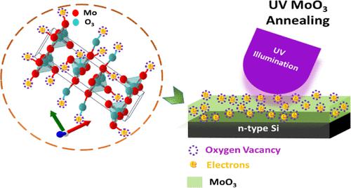
Nanostructures of ultrathin 2D MoO3 semiconductors have gained significant attention in the field of transparent optoelectronics and nanophotonics due to their exceptional responsiveness. In this study, we investigate self-powered α-MoO3/Ir/α-MoO3 photodetectors, focusing on the influence of induced hot electrons in ultrathin α-MoO3 when combined with an ultrathin Ir plasmonic layer. Our results reveal the presence of both positive and negative photoconductivity at a 0 V bias voltage. Notably, by integrating a 2 nm Ir layer between post-annealed α-MoO3 films, we achieve remarkable performance metrics, including a high ION/IOFF ratio of 3.8 × 10⁶, external quantum efficiency of 132, and detectivity of 3.4 × 10¹¹ Jones at 0 V bias. Furthermore, the response time is impressively short, with only 0.2 ms, supported by an exceptionally low MoO3 surface roughness of 0.1 nm. The observed negative photoresponse is attributed to O2 desorption from the MoO3 surface, resulting in increased carrier density and reduced mobility in the Ir layer due to Coulomb trapping and oxygen vacancy deep levels. Consequently, this leads to a decreased carrier mobility and diminished current in the heterostructure. Our findings underscore the enormous potential of ultrathin MoO3 semiconductors for high-performance negative conductivity optoelectronics and photonic applications.
中文翻译:

高性能负自供电 α-MoO3/Ir/α-MoO3 光电探测器:探讨库仑深陷阱的影响
超薄2D MoO 3半导体的纳米结构由于其卓越的响应能力而在透明光电子学和纳米光子学领域获得了极大的关注。在本研究中,我们研究了自供电 α-MoO 3 /Ir/α-MoO 3光电探测器,重点研究与超薄 Ir 等离子体层结合时超薄α-MoO 3中感应热电子的影响。我们的结果揭示了在 0 V 偏置电压下同时存在正光电导性和负光电导性。值得注意的是,通过在退火后的 α-MoO 3薄膜之间集成 2 nm Ir 层,我们实现了卓越的性能指标,包括3.8 × 10 6的高I ON / I OFF比、132 的外量子效率和 3.4 的探测率× 10 11 Jones 在 0 V 偏压下。此外,响应时间非常短,仅为 0.2 ms,这得益于0.1 nm 的极低 MoO 3表面粗糙度。观察到的负光响应归因于O 2从MoO 3表面解吸,导致载流子密度增加,并且由于库仑俘获和氧空位深能级而导致Ir层中的迁移率降低。因此,这导致异质结构中载流子迁移率降低和电流减少。我们的研究结果强调了超薄 MoO 3半导体在高性能负电导率光电和光子应用中的巨大潜力。
更新日期:2023-10-04
中文翻译:
高性能负自供电 α-MoO3/Ir/α-MoO3 光电探测器:探讨库仑深陷阱的影响
超薄2D MoO 3半导体的纳米结构由于其卓越的响应能力而在透明光电子学和纳米光子学领域获得了极大的关注。在本研究中,我们研究了自供电 α-MoO 3 /Ir/α-MoO 3光电探测器,重点研究与超薄 Ir 等离子体层结合时超薄α-MoO 3中感应热电子的影响。我们的结果揭示了在 0 V 偏置电压下同时存在正光电导性和负光电导性。值得注意的是,通过在退火后的 α-MoO 3薄膜之间集成 2 nm Ir 层,我们实现了卓越的性能指标,包括3.8 × 10 6的高I ON / I OFF比、132 的外量子效率和 3.4 的探测率× 10 11 Jones 在 0 V 偏压下。此外,响应时间非常短,仅为 0.2 ms,这得益于0.1 nm 的极低 MoO 3表面粗糙度。观察到的负光响应归因于O 2从MoO 3表面解吸,导致载流子密度增加,并且由于库仑俘获和氧空位深能级而导致Ir层中的迁移率降低。因此,这导致异质结构中载流子迁移率降低和电流减少。我们的研究结果强调了超薄 MoO 3半导体在高性能负电导率光电和光子应用中的巨大潜力。


 京公网安备 11010802027423号