Nano Research ( IF 9.5 ) Pub Date : 2023-10-02 , DOI: 10.1007/s12274-023-6180-2
Lu Li , Yalin Peng , Jinpeng Tian , Fanfan Wu , Xiang Guo , Na Li , Wei Yang , Dongxia Shi , Luojun Du , Guangyu Zhang
|
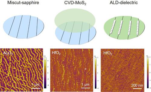
Monolayer molybdenum disulfide (MoS2) has emerged as one of the most promising channel materials for next-generation nanoelectronics and optoelectronics owing to its atomic thickness, dangling-bond-free flat surface, and high electrical quality. Currently, high-quality monolayer MoS2 wafers are primarily grown on sapphire substrates incompatible with conventional device fabrication, and thus transfer processes to a suitable substrate are typically required before the device can be processed. Here, we demonstrate the batch production of transfer-free MoS2 top-gate devices directly on sapphire growth substrates via step engineering. By introducing substrate steps on growth substrate sapphire, high-κ dielectric layers with superior quality and uniform can be directly deposited on the epitaxially grown monolayer MoS2. For the substrate with a maximum step density of 100 µm−1, the gate capacitance can reach ∼ 1.87 µF·cm−2, while the interface trap state density (Dit) can be as low as ∼ 7.6 × 1010 cm−2·eV−1. The direct deposition of high-quality dielectric layers on grown monolayer MoS2 enables the batch fabrication of top-gate devices devoid of transfer and thus excellent device yield of > 96%, holding great promise for large-scale two-dimensional (2D) integrated circuits.
中文翻译:
通过分步工程直接在生长基板上批量制造 MoS2 器件
单层二硫化钼(MoS 2)因其原子厚度、无悬挂键平坦表面和高电质量而成为下一代纳米电子学和光电子学最有前途的通道材料之一。目前,高质量单层MoS 2晶圆主要生长在与传统器件制造不兼容的蓝宝石衬底上,因此在加工器件之前通常需要转移到合适衬底的工艺。在这里,我们演示了通过分步工程直接在蓝宝石生长基板上批量生产无转移 MoS 2顶栅器件。通过在生长衬底蓝宝石上引入衬底步骤,高κ可以在外延生长的单层MoS 2上直接沉积质量优良且均匀的介电层。对于最大台阶密度为100 µm -1 的衬底,栅极电容可以达到~ 1.87 µF·cm -2,而界面陷阱态密度( D it )可以低至~ 7.6 × 10 10 cm -2 。 ·eV -1。在生长的单层 MoS 2上直接沉积高质量介电层可以批量制造无需转移的顶栅器件,从而实现 > 96% 的优异器件良率,为大规模二维 (2D) 集成带来了巨大希望电路。


 京公网安备 11010802027423号