当前位置:
X-MOL 学术
›
ACS Appl. Electron. Mater.
›
论文详情
Our official English website, www.x-mol.net, welcomes your
feedback! (Note: you will need to create a separate account there.)
Electronic Properties and Ballistic Transport Performances of 2D GaO: A DFT-NEGF Study
ACS Applied Electronic Materials ( IF 4.3 ) Pub Date : 2023-09-21 , DOI: 10.1021/acsaelm.3c00919
Jingwen Zhang 1 , Yurong Qin 2 , Wenhan Zhou 1 , Yang Hu 1 , Chuyao Chen 1 , Jialin Yang 1 , Hengze Qu 1 , Xuemin Hu 3
ACS Applied Electronic Materials ( IF 4.3 ) Pub Date : 2023-09-21 , DOI: 10.1021/acsaelm.3c00919
Jingwen Zhang 1 , Yurong Qin 2 , Wenhan Zhou 1 , Yang Hu 1 , Chuyao Chen 1 , Jialin Yang 1 , Hengze Qu 1 , Xuemin Hu 3
Affiliation
|
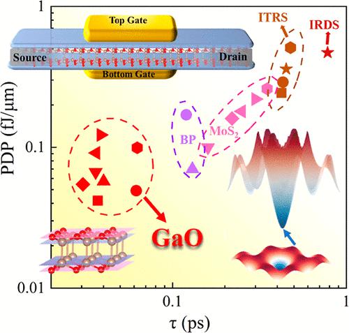
Integrated circuits are the physical foundation of the information society. However, with the development of Moore’s law, silicon-based field-effect transistors (FETs) are approaching their physical limit. Two-dimensional (2D) materials have been classified as highly promising alternative channel materials to silicon due to their extremely thin scale, better gate control properties, and efficient avoidance of short-channel effects. Here, we study the electronic properties of the III–VI 2D semiconductor GaO and its transport properties as a channel material via ab initio simulations. The monolayer GaO has an indirect band gap of 1.57 eV and a small electron effective mass and is relatively stable. The double-gate metal-oxide-semiconductor field-effect transistors (MOSFETs) with 2D GaO as the channel material can still meet the International Technology Roadmap for Semiconductor (ITRS) requirements for high-performance (HP) devices when the channel length is reduced to 4 nm. Moreover, when the channel length is 10 nm, the GaO n-MOSFET not only has a high on-state current of 3923 μA/μm but also has a low subthreshold swing (SS) of 63 mV/dec, which is close to the performance limit. Compared with devices based on other 2D materials, monolayer GaO n-MOSFETs have a smaller delay time (τ) and power-delay product. Therefore, we believe that 2D GaO is a promising channel material for future applications in electronic devices.
中文翻译:

二维 GaO 的电子特性和弹道输运性能:DFT-NEGF 研究
集成电路是信息社会的物理基础。然而,随着摩尔定律的发展,硅基场效应晶体管(FET)正在接近其物理极限。二维(2D)材料因其极薄的尺寸、更好的栅极控制特性以及有效避免短沟道效应而被归类为非常有前途的硅替代沟道材料。在这里,我们通过从头算模拟研究了 III-VI 族二维半导体 GaO 的电子特性及其作为沟道材料的输运特性。单层GaO的间接带隙为1.57 eV,电子有效质量小,相对稳定。以2D GaO为沟道材料的双栅金属氧化物半导体场效应晶体管(MOSFET)在沟道长度减小时仍能满足国际半导体技术路线图(ITRS)对高性能(HP)器件的要求至 4 纳米。此外,当沟道长度为10 nm时,GaO n-MOSFET不仅具有3923 μA/μm的高通态电流,而且还具有63 mV/dec的低亚阈值摆幅(SS),接近于性能限制。与基于其他 2D 材料的器件相比,单层 GaO n-MOSFET 具有更小的延迟时间 (τ) 和功率延迟积。因此,我们相信2D GaO是未来在电子器件中应用的一种有前景的沟道材料。
更新日期:2023-09-21
中文翻译:
二维 GaO 的电子特性和弹道输运性能:DFT-NEGF 研究
集成电路是信息社会的物理基础。然而,随着摩尔定律的发展,硅基场效应晶体管(FET)正在接近其物理极限。二维(2D)材料因其极薄的尺寸、更好的栅极控制特性以及有效避免短沟道效应而被归类为非常有前途的硅替代沟道材料。在这里,我们通过从头算模拟研究了 III-VI 族二维半导体 GaO 的电子特性及其作为沟道材料的输运特性。单层GaO的间接带隙为1.57 eV,电子有效质量小,相对稳定。以2D GaO为沟道材料的双栅金属氧化物半导体场效应晶体管(MOSFET)在沟道长度减小时仍能满足国际半导体技术路线图(ITRS)对高性能(HP)器件的要求至 4 纳米。此外,当沟道长度为10 nm时,GaO n-MOSFET不仅具有3923 μA/μm的高通态电流,而且还具有63 mV/dec的低亚阈值摆幅(SS),接近于性能限制。与基于其他 2D 材料的器件相比,单层 GaO n-MOSFET 具有更小的延迟时间 (τ) 和功率延迟积。因此,我们相信2D GaO是未来在电子器件中应用的一种有前景的沟道材料。


 京公网安备 11010802027423号