当前位置:
X-MOL 学术
›
ACS Appl. Mater. Interfaces
›
论文详情
Our official English website, www.x-mol.net, welcomes your
feedback! (Note: you will need to create a separate account there.)
High-Responsivity and Broadband MoS2 Photodetector Using Interfacial Engineering
ACS Applied Materials & Interfaces ( IF 8.3 ) Pub Date : 2023-09-20 , DOI: 10.1021/acsami.3c09322 Chenglin Wang 1 , Qianqian Wu 1 , Yang Ding 1 , Xiumei Zhang 2 , Wenhui Wang 3 , Xitao Guo 4 , Zhenhua Ni 3 , Liangliang Lin 5 , Zhengyang Cai 1 , Xiaofeng Gu 1 , Shaoqing Xiao 1 , Haiyan Nan 1
ACS Applied Materials & Interfaces ( IF 8.3 ) Pub Date : 2023-09-20 , DOI: 10.1021/acsami.3c09322 Chenglin Wang 1 , Qianqian Wu 1 , Yang Ding 1 , Xiumei Zhang 2 , Wenhui Wang 3 , Xitao Guo 4 , Zhenhua Ni 3 , Liangliang Lin 5 , Zhengyang Cai 1 , Xiaofeng Gu 1 , Shaoqing Xiao 1 , Haiyan Nan 1
Affiliation
|
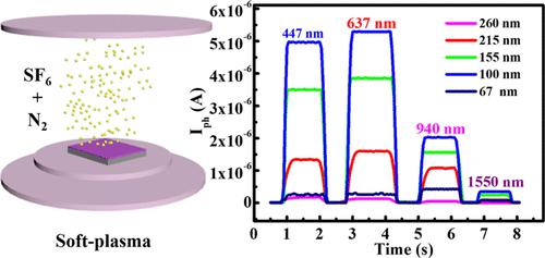
Combining MoS2 with mature silicon technology is an effective method for preparing high-performance photodetectors. However, the previously studied MoS2/silicon-based heterojunction photodetectors cannot simultaneously demonstrate high responsivity, a fast response time, and broad spectral detection. We constructed a broad spectral n-type MoS2/p-type silicon-based heterojunction photodetector. The SiO2 dielectric layer on the silicon substrate was pretreated with soft plasma to change its thickness and surface state. The pretreated SiO2 dielectric layer and the silicon substrate constitute a multilayer heterostructure with a high carrier concentration and responsiveness. Taking silicon-based and n-type MoS2 heterojunction photodetectors as examples, its responsivity can reach 4.05 × 10⁴ A W1– at 637 nm wavelength with a power density of 2 μW mm–2, and the detectable spectral range is measured from 447 to 1600 nm. This pretreated substrate was proven applicable to other n-type TMDCs, such as MoTe2, ReS2, etc., with certain versatility.
中文翻译:

采用界面工程的高响应度和宽带 MoS2 光电探测器
将MoS 2与成熟的硅技术相结合是制备高性能光电探测器的有效方法。然而,先前研究的MoS 2 /硅基异质结光电探测器不能同时表现出高响应率、快速响应时间和宽光谱检测。我们构建了宽光谱n型MoS 2 /p型硅基异质结光电探测器。采用软等离子体对硅衬底上的SiO 2介质层进行预处理,改变其厚度和表面状态。预处理后的SiO 2介质层与硅衬底构成具有高载流子浓度和响应度的多层异质结构。以硅基和n型MoS 2异质结光电探测器为例,其响应度在637 nm波长下可达4.05 × 10 4 AW 1–,功率密度为2 μW mm –2,可检测光谱范围为447至 1600 纳米。该预处理衬底被证明适用于其他n型TMDC,如MoTe 2、ReS 2等,具有一定的通用性。
更新日期:2023-09-20
中文翻译:
采用界面工程的高响应度和宽带 MoS2 光电探测器
将MoS 2与成熟的硅技术相结合是制备高性能光电探测器的有效方法。然而,先前研究的MoS 2 /硅基异质结光电探测器不能同时表现出高响应率、快速响应时间和宽光谱检测。我们构建了宽光谱n型MoS 2 /p型硅基异质结光电探测器。采用软等离子体对硅衬底上的SiO 2介质层进行预处理,改变其厚度和表面状态。预处理后的SiO 2介质层与硅衬底构成具有高载流子浓度和响应度的多层异质结构。以硅基和n型MoS 2异质结光电探测器为例,其响应度在637 nm波长下可达4.05 × 10 4 AW 1–,功率密度为2 μW mm –2,可检测光谱范围为447至 1600 纳米。该预处理衬底被证明适用于其他n型TMDC,如MoTe 2、ReS 2等,具有一定的通用性。


 京公网安备 11010802027423号