当前位置:
X-MOL 学术
›
Adv. Funct. Mater.
›
论文详情
Our official English website, www.x-mol.net, welcomes your
feedback! (Note: you will need to create a separate account there.)
Gate-Last MoS2 Transistors for Active-Matrix Display Driving Circuits
Advanced Functional Materials ( IF 18.5 ) Pub Date : 2023-08-29 , DOI: 10.1002/adfm.202304879
Yalin Peng 1, 2 , Lu Li 1, 2 , Biying Huang 1, 2 , Jinpeng Tian 1, 2 , Xiuzhen Li 1, 2 , Jian Tang 1, 2 , Yanbang Chu 1, 2 , Dongxia Shi 1, 2 , Luojun Du 1, 2 , Na Li 3 , Guangyu Zhang 1, 2, 3
Advanced Functional Materials ( IF 18.5 ) Pub Date : 2023-08-29 , DOI: 10.1002/adfm.202304879
Yalin Peng 1, 2 , Lu Li 1, 2 , Biying Huang 1, 2 , Jinpeng Tian 1, 2 , Xiuzhen Li 1, 2 , Jian Tang 1, 2 , Yanbang Chu 1, 2 , Dongxia Shi 1, 2 , Luojun Du 1, 2 , Na Li 3 , Guangyu Zhang 1, 2, 3
Affiliation
|
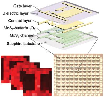
Advancements in display technology have primarily focused on discovering new materials to develop thin-film transistors (TFTs) that complement mainstream technologies. The emerging 2D semiconductors are one of the most promising candidates due to their ultra-thin thickness, exceptional electrical qualities, and large-scale availability. However, these atomically thin materials are delicate and typically prepared through standard gate-first fabrication processes, necessitating their transfer onto specific substrates. In this study, a demonstration of an in situ gate-last process for 2D semiconductor-based TFTs technology is presented. This approach bypasses the yield-limiting transfer process, enabling large-scale display applications. The as-fabricated MoS2 TFTs retains their intrinsic properties with a current density reaching ≈≈10 µA µm−1. Additionally, it is successfully showcased that the two transistor-one capacitor active-matrix display driving circuits with a high pixel yield. The patterned matrix exhibits no crosstalk and can be driven by either the pulse amplitude modulation or pulse width modulation scheme, offering flexible applications.
中文翻译:

用于有源矩阵显示器驱动电路的后栅极 MoS2 晶体管
显示技术的进步主要集中在发现新材料来开发薄膜晶体管 (TFT),以补充主流技术。新兴的二维半导体因其超薄的厚度、卓越的电气质量和大规模可用性而成为最有前途的候选材料之一。然而,这些原子薄材料非常脆弱,通常通过标准的先栅极制造工艺制备,因此需要将它们转移到特定的基板上。在本研究中,演示了基于 2D 半导体的 TFT 技术的原位后栅极工艺。这种方法绕过了产量限制的转移过程,从而实现了大规模显示应用。所制造的MoS 2 TFT保留了其固有特性,电流密度达到约约10 µA µm -1。此外,还成功展示了两种具有高像素良率的晶体管一电容有源矩阵显示驱动电路。图案化矩阵不存在串扰,并且可以通过脉冲幅度调制或脉冲宽度调制方案驱动,提供灵活的应用。
更新日期:2023-08-29
中文翻译:
用于有源矩阵显示器驱动电路的后栅极 MoS2 晶体管
显示技术的进步主要集中在发现新材料来开发薄膜晶体管 (TFT),以补充主流技术。新兴的二维半导体因其超薄的厚度、卓越的电气质量和大规模可用性而成为最有前途的候选材料之一。然而,这些原子薄材料非常脆弱,通常通过标准的先栅极制造工艺制备,因此需要将它们转移到特定的基板上。在本研究中,演示了基于 2D 半导体的 TFT 技术的原位后栅极工艺。这种方法绕过了产量限制的转移过程,从而实现了大规模显示应用。所制造的MoS 2 TFT保留了其固有特性,电流密度达到约约10 µA µm -1。此外,还成功展示了两种具有高像素良率的晶体管一电容有源矩阵显示驱动电路。图案化矩阵不存在串扰,并且可以通过脉冲幅度调制或脉冲宽度调制方案驱动,提供灵活的应用。


 京公网安备 11010802027423号