当前位置:
X-MOL 学术
›
ACS Appl. Nano Mater.
›
论文详情
Our official English website, www.x-mol.net, welcomes your
feedback! (Note: you will need to create a separate account there.)
Density Functional Theory Study of the Electronic and Optical Properties of SnSe2/MoSe2 Heterostructures under Strain and Electric Field: Implications for Optoelectronic Devices
ACS Applied Nano Materials ( IF 5.3 ) Pub Date : 2023-08-25 , DOI: 10.1021/acsanm.3c02635 Yiyu Feng 1 , Hui Bai 2 , Mengya An 2 , Yunkai Wu 1 , Xu Wang 1
ACS Applied Nano Materials ( IF 5.3 ) Pub Date : 2023-08-25 , DOI: 10.1021/acsanm.3c02635 Yiyu Feng 1 , Hui Bai 2 , Mengya An 2 , Yunkai Wu 1 , Xu Wang 1
Affiliation
|
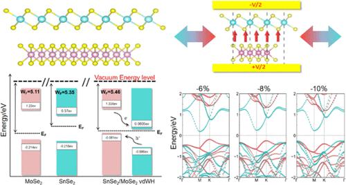
The vertical stacking of various two-dimensional (2D) layered materials to create van der Waals heterostructures (vdWHs) has received great attention as a promising material for developing nanoelectronic and optoelectronic devices. This is because such structures can inherit the unique and favorable properties of a single 2D material. In this study, a SnSe2/MoSe2 vdWH model was built for the first time using the first-principles approach, and its electronic and optical properties were systematically investigated. The results reveal that the SnSe2/MoSe2 vdWH exhibits a type-II heterostructure with a 0.167 eV indirect band gap, which facilitates the separation of photogenerated electron–hole pairs. Notably, the electrical characteristics of the SnSe2/MoSe2 vdWH can be easily controlled by applying an external electric field or biaxial strain. Specifically, a positive electric field or tensile strain narrows the band gap, whereas a negative electric field or compressive strain widens the band gap. The energy band alignment shifts from a type-II to a type-I configuration when a negative electric field of E = −0.6 V Å–1 or a compressive strain of 10% is applied. Furthermore, SnSe2/MoSe2 vdWHs exhibit improved optical absorption across the visible to ultraviolet regions compared to the individual monolayers of SnSe2 and MoSe2. Additionally, the absorption can be influenced by external tension and electric fields. Specifically, under significant compressive strains (10%), the ultraviolet absorption peak reaches 33.5%. Interestingly, a red shift occurs with tensile strain or a negative electric field, whereas a blue shift occurs with compressive strain or a positive electric field. The proposed SnSe2/MoSe2 vdWH in this study offers valuable insights into electronic and optoelectronic device development, particularly in the context of photovoltaic devices, where enhanced ultraviolet absorption can lead to improved light-to-electricity conversion efficiency.
中文翻译:

SnSe2/MoSe2 异质结构在应变和电场下的电子和光学性质的密度泛函理论研究:对光电器件的启示
垂直堆叠各种二维(2D)层状材料以创建范德华异质结构(vdWH)作为开发纳米电子和光电器件的有前途的材料受到了极大的关注。这是因为此类结构可以继承单一二维材料的独特且有利的特性。本研究首次采用第一性原理方法建立了SnSe 2 /MoSe 2 vdWH模型,并系统研究了其电子和光学性质。结果表明,SnSe 2 /MoSe 2vdWH表现出具有0.167 eV间接带隙的II型异质结构,有利于光生电子空穴对的分离。值得注意的是,SnSe 2 /MoSe 2 vdWH的电特性可以通过施加外部电场或双轴应变来容易地控制。具体而言,正电场或拉伸应变使带隙变窄,而负电场或压缩应变使带隙变宽。当施加E = -0.6 V Å –1的负电场或 10% 的压缩应变时,能带排列从 II 型构型转变为 I 型构型。此外,SnSe 2 /MoSe 2与SnSe 2和MoSe 2的单个单层相比,vdWH在可见光到紫外区域表现出改善的光学吸收。此外,吸收可能受到外部张力和电场的影响。具体来说,在显着的压缩应变(10%)下,紫外吸收峰达到33.5%。有趣的是,红移发生在拉伸应变或负电场下,而蓝移发生在压缩应变或正电场下。提出的 SnSe 2 /MoSe 2这项研究中的 vdWH 为电子和光电器件的开发提供了宝贵的见解,特别是在光伏器件中,增强的紫外线吸收可以提高光电转换效率。
更新日期:2023-08-25
中文翻译:
SnSe2/MoSe2 异质结构在应变和电场下的电子和光学性质的密度泛函理论研究:对光电器件的启示
垂直堆叠各种二维(2D)层状材料以创建范德华异质结构(vdWH)作为开发纳米电子和光电器件的有前途的材料受到了极大的关注。这是因为此类结构可以继承单一二维材料的独特且有利的特性。本研究首次采用第一性原理方法建立了SnSe 2 /MoSe 2 vdWH模型,并系统研究了其电子和光学性质。结果表明,SnSe 2 /MoSe 2vdWH表现出具有0.167 eV间接带隙的II型异质结构,有利于光生电子空穴对的分离。值得注意的是,SnSe 2 /MoSe 2 vdWH的电特性可以通过施加外部电场或双轴应变来容易地控制。具体而言,正电场或拉伸应变使带隙变窄,而负电场或压缩应变使带隙变宽。当施加E = -0.6 V Å –1的负电场或 10% 的压缩应变时,能带排列从 II 型构型转变为 I 型构型。此外,SnSe 2 /MoSe 2与SnSe 2和MoSe 2的单个单层相比,vdWH在可见光到紫外区域表现出改善的光学吸收。此外,吸收可能受到外部张力和电场的影响。具体来说,在显着的压缩应变(10%)下,紫外吸收峰达到33.5%。有趣的是,红移发生在拉伸应变或负电场下,而蓝移发生在压缩应变或正电场下。提出的 SnSe 2 /MoSe 2这项研究中的 vdWH 为电子和光电器件的开发提供了宝贵的见解,特别是在光伏器件中,增强的紫外线吸收可以提高光电转换效率。


 京公网安备 11010802027423号