Nano Research ( IF 9.5 ) Pub Date : 2023-08-19 , DOI: 10.1007/s12274-023-6021-3 Cheng Zhang , Biyuan Zheng , Guangcheng Wu , Xueying Liu , Jiaxin Wu , Chengdong Yao , Yizhe Wang , Zilan Tang , Ying Chen , Lizhen Fang , Luying Huang , Dong Li , Shengman Li , Anlian Pan
|
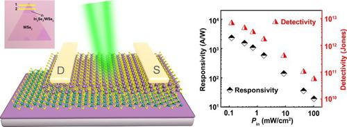
Transition metal dichalcogenides (TMDCs) are promising candidates for future optoelectronic devices accounting for their high carrier mobility and excellent quantum efficiency. However, the limited light absorption efficiency in atomically thin layers significantly hinders photocarrier generation, thereby impairing the optoelectronic performance and hindering practical applications. Herein, we successfully synthesized In2Se3/WSe2 heterostructures through a typical two-step chemical vapor deposition (CVD) method. The In2Se3 nanosheet with strong light absorption capability, serving as the light absorption layer, was integrated with the monolayer WSe2, enhancing the photosensitivity of WSe2 significantly. Upon laser irradiation with a wavelength of 520 nm, the In2Se3/WSe2 heterostructure device shows an ultrahigh photoresponsivity with a value as high as 2333.5 A/W and a remarkable detectivity reaching up to 6.7 × 10¹² Jones, which is the highest among almost the reported TMDCs-based heterostructures grown via CVD even some fabricated by mechanical exfoliation (ME). Combing the advantages of CVD method such as large scale, high yield, and clean interface, the In2Se3/WSe2 heterostructures would provide a novel path for future high-performance optoelectronic device.
中文翻译:

用于超高响应度光电探测器的垂直堆叠 In2Se3/WSe2 异质结构的受控生长
过渡金属二硫属化物(TMDC)因其高载流子迁移率和出色的量子效率而成为未来光电器件的有希望的候选者。然而,原子薄层中有限的光吸收效率显着阻碍了光载流子的产生,从而损害了光电性能并阻碍了实际应用。在此,我们通过典型的两步化学气相沉积(CVD)方法成功合成了In 2 Se 3 /WSe 2异质结构。将具有强光吸收能力的In 2 Se 3纳米片作为光吸收层与单层WSe 2集成在一起,显着增强WSe 2的光敏性。在波长520 nm的激光照射下,In 2 Se 3 /WSe 2异质结构器件表现出高达2333.5 A/W的超高光响应性和高达6.7 × 10 12 Jones的显着探测率。在几乎所有报道的通过 CVD 生长的基于 TMDC 的异质结构中最高,甚至有些是通过机械剥离 (ME) 制造的。结合CVD法大规模、高产率、界面干净等优点,In 2 Se 3 /WSe 2异质结构将为未来高性能光电器件提供一条新途径。














 京公网安备 11010802027423号