当前位置:
X-MOL 学术
›
ACS Appl. Nano Mater.
›
论文详情
Our official English website, www.x-mol.net, welcomes your
feedback! (Note: you will need to create a separate account there.)
A SiGe/Si Nanostructure with Graphene Absorbent for Long Wavelength Infrared Detection
ACS Applied Nano Materials ( IF 5.3 ) Pub Date : 2023-08-17 , DOI: 10.1021/acsanm.3c02607
He Wang 1, 2, 3 , Zhenzhen Kong 2, 3 , Jiale Su 2, 3 , Ben Li 2 , Yijie Wang 2, 3 , Yuanhao Miao 2 , Ziwei Zhou 2 , Xuewei Zhao 2, 3 , Qin Hu 1 , Henry H. Radamson 2
ACS Applied Nano Materials ( IF 5.3 ) Pub Date : 2023-08-17 , DOI: 10.1021/acsanm.3c02607
He Wang 1, 2, 3 , Zhenzhen Kong 2, 3 , Jiale Su 2, 3 , Ben Li 2 , Yijie Wang 2, 3 , Yuanhao Miao 2 , Ziwei Zhou 2 , Xuewei Zhao 2, 3 , Qin Hu 1 , Henry H. Radamson 2
Affiliation
|
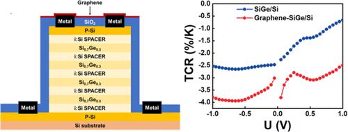
As a representative of new semiconductor nanostructured materials, the Si0.7Ge0.3/Si multilayers have received extensive attention for electronic and photonic applications. We fabricated an uncooled detector consisting of a four-period intrinsic Si0.7Ge0.3/Si multilayer as an active part and two p-type doped electrodes (a PIP profile) for long wavelength infrared detection. The strain in the SiGe/Si multilayer was characterized globally by high-resolution X-ray diffraction (HRXRD) and locally by nanobeam diffraction (NBD) in a high-resolution transmission electron microscope. The performance of detectors was characterized by the temperature coefficient of resistance (TCR), voltage noise power spectral density, and dark current measurement. The detectors with graphene on the top electrode show an improvement for TCR from −2.65%/K to −3.94%/K. Based on our results, the SiGe/Si multilayer structure is an excellent thermal imaging material due to its excellent thermal response as well as its CMOS compatibility.
中文翻译:

用于长波长红外检测的带有石墨烯吸收剂的 SiGe/Si 纳米结构
作为新型半导体纳米结构材料的代表,Si 0.7 Ge 0.3 /Si多层膜在电子和光子应用中受到了广泛的关注。我们制造了一个由四周期本征 Si 0.7 Ge 0.3组成的非冷却探测器/Si 多层作为有源部分和两个 p 型掺杂电极(PIP 轮廓),用于长波长红外检测。SiGe/Si 多层中的应变通过高分辨率 X 射线衍射 (HRXRD) 进行全局表征,并通过高分辨率透射电子显微镜中的纳米束衍射 (NBD) 进行局部表征。探测器的性能通过电阻温度系数 (TCR)、电压噪声功率谱密度和暗电流测量来表征。顶部电极上带有石墨烯的探测器显示 TCR 从 -2.65%/K 提高到 -3.94%/K。根据我们的研究结果,SiGe/Si 多层结构由于其出色的热响应以及 CMOS 兼容性,是一种出色的热成像材料。
更新日期:2023-08-17
中文翻译:
用于长波长红外检测的带有石墨烯吸收剂的 SiGe/Si 纳米结构
作为新型半导体纳米结构材料的代表,Si 0.7 Ge 0.3 /Si多层膜在电子和光子应用中受到了广泛的关注。我们制造了一个由四周期本征 Si 0.7 Ge 0.3组成的非冷却探测器/Si 多层作为有源部分和两个 p 型掺杂电极(PIP 轮廓),用于长波长红外检测。SiGe/Si 多层中的应变通过高分辨率 X 射线衍射 (HRXRD) 进行全局表征,并通过高分辨率透射电子显微镜中的纳米束衍射 (NBD) 进行局部表征。探测器的性能通过电阻温度系数 (TCR)、电压噪声功率谱密度和暗电流测量来表征。顶部电极上带有石墨烯的探测器显示 TCR 从 -2.65%/K 提高到 -3.94%/K。根据我们的研究结果,SiGe/Si 多层结构由于其出色的热响应以及 CMOS 兼容性,是一种出色的热成像材料。


 京公网安备 11010802027423号