当前位置:
X-MOL 学术
›
J. Appl. Crystallogr.
›
论文详情
Our official English website, www.x-mol.net, welcomes your
feedback! (Note: you will need to create a separate account there.)
Thickness independence of antiferroelectric domain characteristic sizes in epitaxial PbZrO3/SrRuO3/SrTiO3 films
Journal of Applied Crystallography ( IF 5.2 ) Pub Date : 2023-05-12 , DOI: 10.1107/s1600576723002868
Jamil Eduardo Flores Gonzales , Alexander Ganzha , Maria Kniazeva , Daria Andronikova , Alexander Vakulenko , Alexei Filimonov , Andrey Rudskoy , Carsten Richter , Arvind Dasgupta , Ran Gao , Roman Burkovsky
|
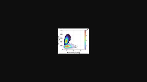
Domain configuration in epitaxial antiferroelectric films has been studied by X-ray nanoscopy, with the extraction of information about the domain sizes beyond the beam-size limit. The objective of this article is to understand how film thickness (the cases of 50 and 1000 nm are explored) and temperature (20 and 200°C) affect the nanodomain configuration of PbZrO3/SrRuO3/SrTiO3 thin films. It is found that the majority of antiferroelectric domains in both films are too small to be directly mappable, because many of them are simultaneously illuminated by the nanobeam (60 × 100 nm) most of the time. Nevertheless, these small sizes can be studied by analysing the diffraction peak width, which is, in the simplest approximation, inversely proportional to the domain size. With this approach it is identified that the characteristic (most probable) domain size does not depend on the film thickness and is ∼13 nm, while the scarcer larger domains do depend on it. An increase of the temperature to 200°C (just below the nominal antiferroelectric-to-cubic transition temperature) results in a slight increase in the characteristic size. These results are compared with those in ferroelectric films, where domain sizes are pronouncedly thickness dependent, and the relevant methodological question on the possibility of neglecting the interference of X-ray waves scattered by different nanodomains in the nanodomain assembly is also discussed.
中文翻译:

外延 PbZrO3/SrRuO3/SrTiO3 薄膜中反铁电畴特征尺寸的厚度独立性
通过 X 射线纳米显微镜研究了外延反铁电薄膜中的畴结构,并提取了有关超出光束尺寸限制的畴尺寸的信息。本文的目的是了解薄膜厚度(探讨了 50 和 1000 nm 的情况)和温度(20 和 200°C)如何影响 PbZrO 3 /SrRuO 3 /SrTiO 3的纳米域配置薄膜。发现两种薄膜中的大多数反铁电畴都太小而无法直接映射,因为其中许多反铁电畴大部分时间都被纳米束 (60 × 100 nm) 同时照射。然而,可以通过分析衍射峰宽来研究这些小尺寸,在最简单的近似中,衍射峰宽与域尺寸成反比。通过这种方法,可以确定特征(最可能的)域大小不取决于薄膜厚度,约为 13 nm,而较稀有的较大域确实取决于它。将温度升高到 200°C(刚好低于标称的反铁电到立方转变温度)会导致特征尺寸略有增加。将这些结果与铁电薄膜中的结果进行比较,
更新日期:2023-05-12
中文翻译:
外延 PbZrO3/SrRuO3/SrTiO3 薄膜中反铁电畴特征尺寸的厚度独立性
通过 X 射线纳米显微镜研究了外延反铁电薄膜中的畴结构,并提取了有关超出光束尺寸限制的畴尺寸的信息。本文的目的是了解薄膜厚度(探讨了 50 和 1000 nm 的情况)和温度(20 和 200°C)如何影响 PbZrO 3 /SrRuO 3 /SrTiO 3的纳米域配置薄膜。发现两种薄膜中的大多数反铁电畴都太小而无法直接映射,因为其中许多反铁电畴大部分时间都被纳米束 (60 × 100 nm) 同时照射。然而,可以通过分析衍射峰宽来研究这些小尺寸,在最简单的近似中,衍射峰宽与域尺寸成反比。通过这种方法,可以确定特征(最可能的)域大小不取决于薄膜厚度,约为 13 nm,而较稀有的较大域确实取决于它。将温度升高到 200°C(刚好低于标称的反铁电到立方转变温度)会导致特征尺寸略有增加。将这些结果与铁电薄膜中的结果进行比较,


 京公网安备 11010802027423号