当前位置:
X-MOL 学术
›
Adv. Mater. Technol.
›
论文详情
Our official English website, www.x-mol.net, welcomes your
feedback! (Note: you will need to create a separate account there.)
Weak Light-Stimulated Synaptic Transistors Based on MoS2/Organic Semiconductor Heterojunction for Neuromorphic Computing
Advanced Materials Technologies ( IF 6.4 ) Pub Date : 2023-05-16 , DOI: 10.1002/admt.202300449
Jun Wang 1 , Ben Yang 1 , Shilei Dai 1 , Pu Guo 1 , Yushan Gao 1 , Li Li 1 , Ziyi Guo 1 , Junyao Zhang 1 , Jianhua Zhang 2 , Jia Huang 1, 3
Advanced Materials Technologies ( IF 6.4 ) Pub Date : 2023-05-16 , DOI: 10.1002/admt.202300449
Jun Wang 1 , Ben Yang 1 , Shilei Dai 1 , Pu Guo 1 , Yushan Gao 1 , Li Li 1 , Ziyi Guo 1 , Junyao Zhang 1 , Jianhua Zhang 2 , Jia Huang 1, 3
Affiliation
|
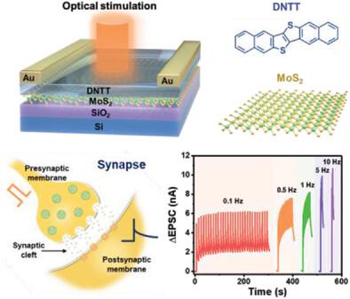
Photonic synapses are expected to play an important role in implementing brain-like computing owing to the wide bandwidth and low mutual interference of optical signals. Herein, photonic synaptic transistors based on inorganic semiconductor molybdenum disulfide (MoS2) and organic semiconductor heterojunction with adjustable short-term/long-term plasticity are proposed. Benefitting from the outstanding photosensitive characteristics originating from the heterojunction, the devices have the capability of weak light detection and can exhibit distinct synaptic responses even under an ultraweak light intensity of 40 nW cm−2, which is considerably lower than that of most previously reported photonic synaptic transistors. Furthermore, a low energy consumption of 0.4 fJ per synaptic event can be obtained at a low operating voltage of 0.001 V, lower than that required for a single synaptic event observed in human brains. In addition, the devices can implement high-pass filtering function and illustrate the potential in image sharpening processing. More significantly, logic functions as well as associative learning behavior are dramatically simulated through all-optical stimulation. This work demonstrates a feasible approach to developing multifunctional photonic synaptic transistors based on inorganic/organic semiconductor heterojunction for neuromorphic computing.
中文翻译:

用于神经形态计算的基于MoS2/有机半导体异质结的弱光刺激突触晶体管
由于光信号的宽带宽和低相互干扰,光子突触有望在实现类脑计算中发挥重要作用。在此,提出了基于无机半导体二硫化钼(MoS2)和具有可调节的短期/长期可塑性的有机半导体异质结的光子突触晶体管。得益于异质结优异的光敏特性,该器件具有弱光检测能力,即使在40 nW cm -2 的超弱光强度下也能表现出明显的突触反应,这比之前报道的大多数光子突触晶体管要低得多。此外,在0.001 V的低工作电压下可以获得每个突触事件0.4 fJ的低能耗,低于在人脑中观察到的单个突触事件所需的能量消耗。此外,该器件还可以实现高通滤波功能,展示了图像锐化处理的潜力。更重要的是,逻辑功能以及联想学习行为通过全光刺激得到了戏剧性的模拟。这项工作展示了一种开发基于无机/有机半导体异质结的多功能光子突触晶体管用于神经形态计算的可行方法。
更新日期:2023-05-16
中文翻译:
用于神经形态计算的基于MoS2/有机半导体异质结的弱光刺激突触晶体管
由于光信号的宽带宽和低相互干扰,光子突触有望在实现类脑计算中发挥重要作用。在此,提出了基于无机半导体二硫化钼(MoS2)和具有可调节的短期/长期可塑性的有机半导体异质结的光子突触晶体管。得益于异质结优异的光敏特性,该器件具有弱光检测能力,即使在40 nW cm -2 的超弱光强度下也能表现出明显的突触反应,这比之前报道的大多数光子突触晶体管要低得多。此外,在0.001 V的低工作电压下可以获得每个突触事件0.4 fJ的低能耗,低于在人脑中观察到的单个突触事件所需的能量消耗。此外,该器件还可以实现高通滤波功能,展示了图像锐化处理的潜力。更重要的是,逻辑功能以及联想学习行为通过全光刺激得到了戏剧性的模拟。这项工作展示了一种开发基于无机/有机半导体异质结的多功能光子突触晶体管用于神经形态计算的可行方法。


 京公网安备 11010802027423号