Applied Surface Science ( IF 6.3 ) Pub Date : 2023-05-12 , DOI: 10.1016/j.apsusc.2023.157489
Chao-Ching Chiang , Xinyi Xia , Jian-Sian Li , Fan Ren , S.J. Pearton
|
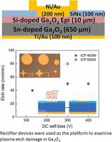
The β-polytype of Ga2O3 has a high critical electric field strength (∼8 MV.cm−1) and can be grown as large diameter (6 in.) single crystal boules by inexpensive melt-growth techniques. This makes it promising for next generation power electronics and solar-blind UV photodetectors. Since wet etching is not feasible for patterning such devices due to the chemical inertness of Ga2O3, attention is focused on dry etching, with the attendant issue of surface modification due to chemical or ion-induced changes. In this work, we demonstrate that dry etch damage in β-Ga2O3 is manifested by a reduction in near-surface carrier concentration, possibly due to the introduction of Gav acceptor states. The depth to which the carrier density is affected depends on the interplay between ion energy and etch rate, with faster etch rates reducing the depth of the remaining damaged region. The maximum damage depth observed experimentally from capacitance-voltage profiling on Schottky rectifiers was ∼ 110 nm, well beyond the range of the ions in the Inductively Coupled Plasmas and emphasizing that rapid diffusion of point defects occurs into the sample during the etch step. Using Schottky rectifier structures as a platform to understand the effect of dry etch damage on device parameters, we found that on-state resistance was more affected than ideality factor or breakdown voltage, with a large increase (5x) for ion energies ≥ 325 eV. Reverse current density characteristics showed the presence of trap-assisted space-charge-limited conduction in the damaged layers. The implications for high power rectifier fabrication are discussed.
中文翻译:
Ga2O3 肖特基整流器中干蚀刻损伤深度的离子能量依赖性
Ga 2 O 3的β-多型体具有高临界电场强度(~8 MV.cm -1)并且可以通过廉价的熔体生长技术生长为大直径(6 英寸)单晶晶锭。这使得它有望用于下一代电力电子和日盲紫外光电探测器。由于 Ga 2 O 3的化学惰性,湿法蚀刻不适用于图案化此类器件,因此注意力集中在干法蚀刻上,伴随着由于化学或离子引起的变化而导致的表面改性问题。在这项工作中,我们证明了 β-Ga 2 O 3中的干法蚀刻损伤表现为近表面载流子浓度的降低,这可能是由于 Ga v的引入受体状态。载流子密度受影响的深度取决于离子能量和蚀刻速率之间的相互作用,更快的蚀刻速率会减少剩余损坏区域的深度。从肖特基整流器的电容电压曲线实验中观察到的最大损伤深度约为 110 nm,远远超出电感耦合等离子体中离子的范围,并强调点缺陷在蚀刻步骤中会快速扩散到样品中。使用肖特基整流器结构作为平台来了解干法刻蚀损伤对器件参数的影响,我们发现导通电阻比理想因子或击穿电压受到的影响更大,离子能量 ≥ 325 eV 时会大幅增加 (5x)。反向电流密度特性表明在受损层中存在陷阱辅助空间电荷限制传导。讨论了对大功率整流器制造的影响。


 京公网安备 11010802027423号