Surfaces and Interfaces ( IF 5.7 ) Pub Date : 2023-04-26 , DOI: 10.1016/j.surfin.2023.102892
S Sadhasivam , N Anbarasan , A Gunasekaran , T Sadhasivam , K Jeganathan , T H Oh
|
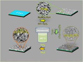
Highly efficient visible light excitation and generating high photogenerated charges in semiconductor electrodes yet challenging in photoelectrochemical (PEC) water splitting. Herein, dual heterojunctions comprising of WO3/Bi2WO6 2D nanoflakes surrounded by In2S3 nanosphere photo absorbers used as a photoelectrodes. Under visible light irradiation, the WO3/Bi2WO6/In2S3 photoelectrode produced an excellent low overpotential-photocurrent. The photocurrent density of 4.02 mA/cm2 at 0.84 V vs. RHE was achieved for a heterostructure photoanode and 8-fold higher than WO3 photoanode. The incident photon to the current conversion efficiency of WO3/Bi2WO6/In2S3 (52% at 400 nm) is about 8 fold higher that of WO3. The improved hydrogen evolution performance was attained through hindering recombination and better band alignment between In2S3 and Bi2WO6. The low charge transfer resistance (152.8 Ohm) of WO3/Bi2WO6/In2S3 photoanode substantially improves the surface charge separation through In2S3 photoactivated catalytic sites. The WO3/Bi2WO6/In2S3 photoanode demonstrates an outstanding charge carriers lifetime, resulting in a maximum photocurrent density of 4.02 mA/cm2 for stable water splitting applications.
中文翻译:
高效 In2S3 纳米球装饰 WO3/Bi2WO6 双异质结构纳米片阵列,用于增强可见光照射下的低偏水分解
高效可见光激发并在半导体电极中产生高光生电荷,但在光电化学 (PEC) 水分解中具有挑战性。在此,包含被 In 2 S 3纳米球光吸收剂包围的 WO 3 /Bi 2 WO 6 2D 纳米薄片的双异质结用作光电极。在可见光照射下,WO 3 /Bi 2 WO 6 /In 2 S 3光电极产生了优异的低过电势-光电流。4.02 mA/cm 2的光电流密度异质结构光电阳极的电压为 0.84 V vs. RHE,比 WO 3光电阳极高 8 倍。WO 3 /Bi 2 WO 6 /In 2 S 3的入射光子到电流的转换效率(在400nm处为52%)比WO 3高约8倍。通过阻碍 In 2 S 3和 Bi 2 WO 6之间的重组和更好的带排列,实现了改进的析氢性能。WO 3 /Bi 2 WO 6 /In 2 S 3的低电荷转移电阻(152.8 Ohm)光电阳极通过 In 2 S 3光活化催化位点显着改善表面电荷分离。WO 3 /Bi 2 WO 6 /In 2 S 3光电阳极展示了出色的载流子寿命,导致稳定的水分解应用的最大光电流密度为 4.02 mA/cm 2。


 京公网安备 11010802027423号