当前位置:
X-MOL 学术
›
ACS Appl. Mater. Interfaces
›
论文详情
Our official English website, www.x-mol.net, welcomes your
feedback! (Note: you will need to create a separate account there.)
Physical Properties of an Ultrathin Al2O3/HfO2 Composite Film by Atomic Layer Deposition and the Application in Thin-Film Transistors
ACS Applied Materials & Interfaces ( IF 8.3 ) Pub Date : 2023-03-21 , DOI: 10.1021/acsami.2c22227
Yachen Xu 1 , Huimin Chen 1 , Haiyang Xu 2 , Minyu Chen 1, 3 , Pengchao Zhou 1 , Shuzhe Li 1 , Ge Zhang 4 , Wei Shi 2 , Xuyong Yang 1 , Xingwei Ding 2 , Bin Wei 1, 2
ACS Applied Materials & Interfaces ( IF 8.3 ) Pub Date : 2023-03-21 , DOI: 10.1021/acsami.2c22227
Yachen Xu 1 , Huimin Chen 1 , Haiyang Xu 2 , Minyu Chen 1, 3 , Pengchao Zhou 1 , Shuzhe Li 1 , Ge Zhang 4 , Wei Shi 2 , Xuyong Yang 1 , Xingwei Ding 2 , Bin Wei 1, 2
Affiliation
|
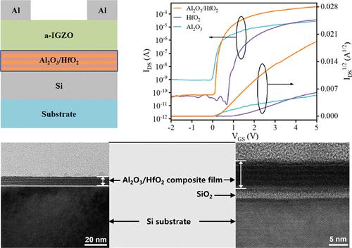
A high-quality ultrathin dielectric film is important in the field of microelectronics. We designed a composite structure composed of Al2O3/HfO2 with different Al2O3/HfO2 cycles prepared by atomic layer deposition (ALD) to obtain high-quality ultrathin (1–12 nm) dielectric films. Al2O3 protected HfO2 from interacting with the Si substrate and inhibited the crystallization of the HfO2 film. High permittivity material of HfO2 was adopted to guarantee the good insulating property of the composite film. We investigated the physical properties as well as the growth mode of the composite film and found that the film exhibited a layer growth mode. The water contact angle and grazing-incidence small-angle X-ray scattering analyses revealed that the film was formed physically at 3 nm, while the thickness of the electrically stable film was 10 nm from grazing-incidence wide-angle X-ray scattering and dielectric constant analyses. The composite film was applied as a dielectric layer in thin-film transistors (TFTs). The threshold voltage was decreased to 0.27 V compared to the organic field-effect transistor with the single HfO2 dielectric, and the subthreshold swing was as small as 0.05 V/dec with a carrier mobility of 49.2 cm2/V s. The off-current was as low as 10–11 A, and the on/off ratio was as high as 5.5 × 10⁶. This ALD-prepared composite strategy provides a simple and practical way to obtain the high-quality dielectric film, which shows the potential application in the field of microelectronics.
中文翻译:

原子层沉积超薄Al2O3/HfO2复合薄膜的物理性质及其在薄膜晶体管中的应用
高质量的超薄介电薄膜在微电子领域具有重要意义。我们设计了一种由具有不同Al 2 O 3 /HfO 2循环的Al 2 O 3 /HfO 2组成的复合结构,通过原子层沉积(ALD)制备以获得高质量的超薄(1-12 nm)介电薄膜。Al 2 O 3保护HfO 2不与Si衬底相互作用并抑制HfO 2膜的结晶。HfO 2高介电材料以保证复合薄膜良好的绝缘性能。我们研究了复合薄膜的物理性质和生长模式,发现该薄膜呈层状生长模式。水接触角和掠入射小角 X 射线散射分析表明,薄膜物理形成为 3 nm,而电稳定薄膜的厚度为 10 nm,来自掠入射广角 X 射线散射和介电常数分析。该复合膜被用作薄膜晶体管 (TFT) 中的介电层。与具有单一 HfO 2电介质的有机场效应晶体管相比,阈值电压降至 0.27 V,亚阈值摆幅小至 0.05 V/dec,载流子迁移率为 49.2 cm2 /V 秒。关断电流低至 10 –11 A,开/关比高达 5.5 × 10 6。这种 ALD 制备的复合策略为获得高质量介电薄膜提供了一种简单实用的方法,显示出在微电子领域的潜在应用。
更新日期:2023-03-21
中文翻译:
原子层沉积超薄Al2O3/HfO2复合薄膜的物理性质及其在薄膜晶体管中的应用
高质量的超薄介电薄膜在微电子领域具有重要意义。我们设计了一种由具有不同Al 2 O 3 /HfO 2循环的Al 2 O 3 /HfO 2组成的复合结构,通过原子层沉积(ALD)制备以获得高质量的超薄(1-12 nm)介电薄膜。Al 2 O 3保护HfO 2不与Si衬底相互作用并抑制HfO 2膜的结晶。HfO 2高介电材料以保证复合薄膜良好的绝缘性能。我们研究了复合薄膜的物理性质和生长模式,发现该薄膜呈层状生长模式。水接触角和掠入射小角 X 射线散射分析表明,薄膜物理形成为 3 nm,而电稳定薄膜的厚度为 10 nm,来自掠入射广角 X 射线散射和介电常数分析。该复合膜被用作薄膜晶体管 (TFT) 中的介电层。与具有单一 HfO 2电介质的有机场效应晶体管相比,阈值电压降至 0.27 V,亚阈值摆幅小至 0.05 V/dec,载流子迁移率为 49.2 cm2 /V 秒。关断电流低至 10 –11 A,开/关比高达 5.5 × 10 6。这种 ALD 制备的复合策略为获得高质量介电薄膜提供了一种简单实用的方法,显示出在微电子领域的潜在应用。


 京公网安备 11010802027423号