当前位置:
X-MOL 学术
›
Nanoscale Horiz.
›
论文详情
Our official English website, www.x-mol.net, welcomes your
feedback! (Note: you will need to create a separate account there.)
C3N2: the missing part of highly stable porous graphitic carbon nitride semiconductors
Nanoscale Horizons ( IF 8.0 ) Pub Date : 2023-03-07 , DOI: 10.1039/d2nh00440b
Xinyong Cai 1 , Jiao Chen 1 , Hongyan Wang 1 , Yuxiang Ni 1 , Yuanzheng Chen 1, 2 , R Bruce King 3
Nanoscale Horizons ( IF 8.0 ) Pub Date : 2023-03-07 , DOI: 10.1039/d2nh00440b
Xinyong Cai 1 , Jiao Chen 1 , Hongyan Wang 1 , Yuxiang Ni 1 , Yuanzheng Chen 1, 2 , R Bruce King 3
Affiliation
|
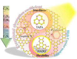
Two-dimensional (2D) porous graphitic carbon nitrides (PGCNs) with semiconducting features have attracted wide attention because of built-in pores with various active sites, large surface area, and high physicochemical stability. However, only a few PGCNs have been synthesized, covering a 1.23–3.18 eV band gap. We systematically investigate two new 2D PGCN monolayers, T-C3N2 and H-C3N2, including possible pathways for their experimental synthesis. Based on first-principles calculations, the mechanical, electronic, and optical properties of T-C3N2 and H-C3N2 have been systematically investigated. These two architectural frameworks exhibit contrasting mechanical characteristics owing to their structural differences. Both T-C3N2 and H-C3N2 monolayers are predicted to be intrinsic semiconductors. Exceptionally, the stacking bilayers of T-C3N2 can transform into a rare 2D nodal-line semimetal structure. The narrow bandgap (0.35 eV) of the T-C3N2 monolayer and its extraordinary transformation in the bilayer electronic structure fill the vacancy of PGCNs as electronic devices in the middle/long wave infrared region. C3N2 structures possess ultrahigh anisotropic carrier mobilities (×104 cm2 V−1 s−1) and exceptional absorption coefficients (×105 cm−1) in the near-infrared and visible light regions, suggesting its possible optoelectronic applications. The findings expand the scope of 2D PGCNs and offer guides for their experimental realization.
中文翻译:

C3N2:高稳定性多孔石墨氮化碳半导体的缺失部分
具有半导体特性的二维 (2D) 多孔石墨碳氮化物 (PGCNs) 因其具有多种活性位点、大表面积和高物理化学稳定性的内置孔而受到广泛关注。然而,只有少数 PGCN 被合成,覆盖了 1.23-3.18 eV 的带隙。我们系统地研究了两种新的 2D PGCN 单层膜,TC 3 N 2和 HC 3 N 2,包括它们的实验合成的可能途径。基于第一性原理计算,TC 3 N 2和HC 3 N 2的机械、电子和光学性质进行了系统的调查。由于它们的结构差异,这两种架构框架表现出截然不同的机械特性。预计TC 3 N 2和 HC 3 N 2单层都是本征半导体。例外的是,TC 3 N 2的堆叠双层可以转变为罕见的二维节点线半金属结构。TC 3 N 2单分子层的窄带隙(0.35 eV)及其在双层电子结构中的非凡转变填补了PGCNs作为中/长波红外区电子器件的空缺。碳3氮2结构在近红外和可见光区域具有超高各向异性载流子迁移率 (×10 4 cm 2 V -1 s -1 ) 和出色的吸收系数 (×10 5 cm -1 ),表明其可能的光电应用。这些发现扩大了 2D PGCN 的范围,并为其实验实现提供了指导。
更新日期:2023-03-07
中文翻译:
C3N2:高稳定性多孔石墨氮化碳半导体的缺失部分
具有半导体特性的二维 (2D) 多孔石墨碳氮化物 (PGCNs) 因其具有多种活性位点、大表面积和高物理化学稳定性的内置孔而受到广泛关注。然而,只有少数 PGCN 被合成,覆盖了 1.23-3.18 eV 的带隙。我们系统地研究了两种新的 2D PGCN 单层膜,TC 3 N 2和 HC 3 N 2,包括它们的实验合成的可能途径。基于第一性原理计算,TC 3 N 2和HC 3 N 2的机械、电子和光学性质进行了系统的调查。由于它们的结构差异,这两种架构框架表现出截然不同的机械特性。预计TC 3 N 2和 HC 3 N 2单层都是本征半导体。例外的是,TC 3 N 2的堆叠双层可以转变为罕见的二维节点线半金属结构。TC 3 N 2单分子层的窄带隙(0.35 eV)及其在双层电子结构中的非凡转变填补了PGCNs作为中/长波红外区电子器件的空缺。碳3氮2结构在近红外和可见光区域具有超高各向异性载流子迁移率 (×10 4 cm 2 V -1 s -1 ) 和出色的吸收系数 (×10 5 cm -1 ),表明其可能的光电应用。这些发现扩大了 2D PGCN 的范围,并为其实验实现提供了指导。


 京公网安备 11010802027423号