Our official English website, www.x-mol.net, welcomes your
feedback! (Note: you will need to create a separate account there.)
Introduction of defects in hexagonal boron nitride for vacancy-based 2D memristors
Nanoscale ( IF 5.8 ) Pub Date : 2023-02-09 , DOI: 10.1039/d2nr07234c Haohan Chen 1, 2 , Yu Kang 2 , Dong Pu 2 , Ming Tian 3 , Neng Wan 3 , Yang Xu 2 , Bin Yu 2 , Wenjing Jie 1 , Yuda Zhao 2
Nanoscale ( IF 5.8 ) Pub Date : 2023-02-09 , DOI: 10.1039/d2nr07234c Haohan Chen 1, 2 , Yu Kang 2 , Dong Pu 2 , Ming Tian 3 , Neng Wan 3 , Yang Xu 2 , Bin Yu 2 , Wenjing Jie 1 , Yuda Zhao 2
Affiliation
|
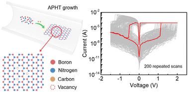
Two-dimensional (2D) materials have become potential resistive switching (RS) layers to prepare emerging non-volatile memristors. The atomically thin thickness and the highly controllable defect density contribute to the construction of ultimately scaled memory cells with stable switching behaviors. Although the conductive bridge random-access memory based on 2D hexagonal boron nitride has been widely studied, the realization of RS completely relying on vacancies in 2D materials has performance superiority. Here, we synthesize carbon-doped h-BN (C-h-BN) with a certain number of defects by controlling the weight percentage of carbon powder in the source. These defects can form a vacancy-based conductive filament under an applied electric field. The memristor displays bipolar non-volatile memory with a low SET voltage of 0.85 V and shows a long retention time of up to 104 s at 120 °C. The response times of the SET and RESET process are less than 80 ns and 240 ns, respectively. The current mapping by conductive atomic force microscopy demonstrates the electric-field-induced current tunneling from defective sites of the C-h-BN flake, revealing the defect-based RS in the C-h-BN memristor. Moreover, C-h-BN with excellent flexibility can be applied to wearable devices, maintaining stable RS performance in a variety of bending environments and after multiple bending cycles. The vacancy-based 2D memristor provides a new strategy for developing ultra-scaled memory units with high controllability.
中文翻译:

用于基于空位的二维忆阻器的六方氮化硼缺陷介绍
二维 (2D) 材料已成为潜在的电阻开关 (RS) 层,用于制备新兴的非易失性忆阻器。原子级薄的厚度和高度可控的缺陷密度有助于构建具有稳定开关行为的最终缩放存储单元。尽管基于二维六方氮化硼的导电桥随机存取存储器已被广泛研究,但完全依靠二维材料中的空位实现RS具有性能优势。在这里,我们通过控制源中碳粉的重量百分比,合成了具有一定数量缺陷的碳掺杂 h-BN (Ch-BN)。这些缺陷可以在施加的电场下形成基于空位的导电丝。忆阻器显示双极非易失性存储器,低 SET 电压为 0。120 °C 时4秒。SET 和 RESET 过程的响应时间分别小于 80 ns 和 240 ns。通过导电原子力显微镜进行的电流映射证明了 Ch-BN 薄片缺陷部位的电场感应电流隧穿,揭示了 Ch-BN 忆阻器中基于缺陷的 RS。此外,具有优异柔韧性的 Ch-BN 可应用于可穿戴设备,在各种弯曲环境和多次弯曲循环后保持稳定的 RS 性能。基于空位的二维忆阻器为开发具有高可控性的超大规模存储单元提供了一种新策略。
更新日期:2023-02-09
中文翻译:
用于基于空位的二维忆阻器的六方氮化硼缺陷介绍
二维 (2D) 材料已成为潜在的电阻开关 (RS) 层,用于制备新兴的非易失性忆阻器。原子级薄的厚度和高度可控的缺陷密度有助于构建具有稳定开关行为的最终缩放存储单元。尽管基于二维六方氮化硼的导电桥随机存取存储器已被广泛研究,但完全依靠二维材料中的空位实现RS具有性能优势。在这里,我们通过控制源中碳粉的重量百分比,合成了具有一定数量缺陷的碳掺杂 h-BN (Ch-BN)。这些缺陷可以在施加的电场下形成基于空位的导电丝。忆阻器显示双极非易失性存储器,低 SET 电压为 0。120 °C 时4秒。SET 和 RESET 过程的响应时间分别小于 80 ns 和 240 ns。通过导电原子力显微镜进行的电流映射证明了 Ch-BN 薄片缺陷部位的电场感应电流隧穿,揭示了 Ch-BN 忆阻器中基于缺陷的 RS。此外,具有优异柔韧性的 Ch-BN 可应用于可穿戴设备,在各种弯曲环境和多次弯曲循环后保持稳定的 RS 性能。基于空位的二维忆阻器为开发具有高可控性的超大规模存储单元提供了一种新策略。


 京公网安备 11010802027423号