当前位置:
X-MOL 学术
›
ACS Appl. Mater. Interfaces
›
论文详情
Our official English website, www.x-mol.net, welcomes your
feedback! (Note: you will need to create a separate account there.)
Characterizing Density and Spatial Distribution of Trap States in Ta3N5 Thin Films for Rational Defect Passivation
ACS Applied Materials & Interfaces ( IF 8.3 ) Pub Date : 2023-02-03 , DOI: 10.1021/acsami.2c19275
Peter N Rudd 1 , Stephen J Tereniak 2 , Rene Lopez 1, 3
ACS Applied Materials & Interfaces ( IF 8.3 ) Pub Date : 2023-02-03 , DOI: 10.1021/acsami.2c19275
Peter N Rudd 1 , Stephen J Tereniak 2 , Rene Lopez 1, 3
Affiliation
|
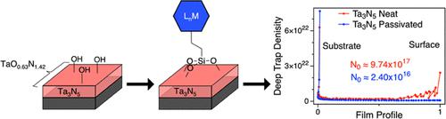
Tantalum nitride (Ta3N5) has gained significant attention as a potential photoanode material, yet it has been challenged by material quality issues. Defect-induced trap states are detrimental to the performance of any semiconductor material. Beyond influencing the performance of Ta3N5 films, defects can also accelerate the degradation in water during desired electrochemical applications. Defect passivation has provided an enormous boost to the development of many semiconductor materials but is currently in its infancy for Ta3N5. This is in part due to a lack of experimental understanding regarding the spatial and energetic distribution of trap states throughout Ta3N5 thin films. Here, we employ drive-level capacitance profiling (DLCP) to experimentally resolve the spatial and energetic distribution of trap states throughout Ta3N5 thin films. The density of deeper energetic traps is found to reach ∼2.5 to 6 × 1022 cm–3 at the interfaces of neat Ta3N5 thin films, over an order of magnitude greater than the bulk. In addition to the spatial profile of deep trap states, we report neat Ta3N5 thin films to be highly n-type in nature, owning a free carrier density of ∼9.74 × 1017 cm–3. This information, coupled with the present understanding of native oxide layers on Ta3N5, has facilitated the rational design of a targeted passivation strategy that simultaneously provides a means for catalyst immobilization. Loading catalyst via silatrane moieties suppresses the density of defects at the surface of Ta3N5 thin films by two orders of magnitude, while also reducing the free carrier density of films by over one order of magnitude, effectively dedoping the films to ∼2.40 × 1016 cm–3. The surface passivation of Ta3N5 films translates to suppressed defect-induced trapping and recombination of photoexcited carriers, as determined through absorption, photoluminescence, and transient photovoltage. This illustrates how developing a deeper understanding of the distribution and influence of defects in Ta3N5 thin films has the potential to guide future works and ultimately accelerate the integration and development of high-performance Ta3N5 thin film devices.
中文翻译:

表征 Ta3N5 薄膜中陷阱态的密度和空间分布以进行合理的缺陷钝化
氮化钽 (Ta 3 N 5 ) 作为一种潜在的光电阳极材料受到了广泛关注,但它一直受到材料质量问题的挑战。缺陷诱导的陷阱态对任何半导体材料的性能都是有害的。除了影响 Ta 3 N 5薄膜的性能外,缺陷还会在所需的电化学应用过程中加速水中的降解。缺陷钝化极大地推动了许多半导体材料的发展,但目前 Ta 3 N 5还处于起步阶段。这部分是由于缺乏对整个 Ta 3陷阱态的空间和能量分布的实验理解N 5薄膜。在这里,我们采用驱动级电容分布 (DLCP) 来通过实验解决整个 Ta 3 N 5薄膜中陷阱态的空间和能量分布。在纯 Ta 3 N 5薄膜的界面处,发现更深的能量陷阱的密度达到 ∼2.5 至 6 × 10 22 cm –3,比体积大一个数量级。除了深陷阱态的空间分布外,我们还报告了纯 Ta 3 N 5薄膜本质上是高度 n 型的,拥有约 9.74 × 10 17 cm –3的自由载流子密度. 该信息,加上目前对 Ta 3 N 5上自然氧化层的理解,促进了目标钝化策略的合理设计,同时提供了一种催化剂固定方法。通过硅烷部分负载催化剂将 Ta 3 N 5薄膜表面的缺陷密度抑制了两个数量级,同时也将薄膜的自由载流子密度降低了一个数量级以上,有效地将薄膜去掺杂至~2.40 × 10 16厘米–3。Ta 3 N 5的表面钝化薄膜转化为抑制缺陷诱导的光激发载流子的捕获和重组,如通过吸收、光致发光和瞬态光电压所确定的。这说明了对 Ta 3 N 5薄膜中缺陷的分布和影响的更深入理解如何有可能指导未来的工作并最终加速高性能 Ta 3 N 5薄膜器件的集成和开发。
更新日期:2023-02-03
中文翻译:
表征 Ta3N5 薄膜中陷阱态的密度和空间分布以进行合理的缺陷钝化
氮化钽 (Ta 3 N 5 ) 作为一种潜在的光电阳极材料受到了广泛关注,但它一直受到材料质量问题的挑战。缺陷诱导的陷阱态对任何半导体材料的性能都是有害的。除了影响 Ta 3 N 5薄膜的性能外,缺陷还会在所需的电化学应用过程中加速水中的降解。缺陷钝化极大地推动了许多半导体材料的发展,但目前 Ta 3 N 5还处于起步阶段。这部分是由于缺乏对整个 Ta 3陷阱态的空间和能量分布的实验理解N 5薄膜。在这里,我们采用驱动级电容分布 (DLCP) 来通过实验解决整个 Ta 3 N 5薄膜中陷阱态的空间和能量分布。在纯 Ta 3 N 5薄膜的界面处,发现更深的能量陷阱的密度达到 ∼2.5 至 6 × 10 22 cm –3,比体积大一个数量级。除了深陷阱态的空间分布外,我们还报告了纯 Ta 3 N 5薄膜本质上是高度 n 型的,拥有约 9.74 × 10 17 cm –3的自由载流子密度. 该信息,加上目前对 Ta 3 N 5上自然氧化层的理解,促进了目标钝化策略的合理设计,同时提供了一种催化剂固定方法。通过硅烷部分负载催化剂将 Ta 3 N 5薄膜表面的缺陷密度抑制了两个数量级,同时也将薄膜的自由载流子密度降低了一个数量级以上,有效地将薄膜去掺杂至~2.40 × 10 16厘米–3。Ta 3 N 5的表面钝化薄膜转化为抑制缺陷诱导的光激发载流子的捕获和重组,如通过吸收、光致发光和瞬态光电压所确定的。这说明了对 Ta 3 N 5薄膜中缺陷的分布和影响的更深入理解如何有可能指导未来的工作并最终加速高性能 Ta 3 N 5薄膜器件的集成和开发。


 京公网安备 11010802027423号