Light: Science & Applications ( IF 20.6 ) Pub Date : 2023-01-24 , DOI: 10.1038/s41377-022-01037-7 Xiufang Chen 1 , Xianglong Yang 1 , Xuejian Xie 1 , Yan Peng 1 , Longfei Xiao 1 , Chen Shao 1 , Huadong Li 1 , Xiaobo Hu 1 , Xiangang Xu 1
|
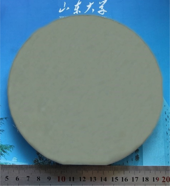
SiC semiconductor is the focus of recent international research. It is also an important raw material for China to achieve carbon emission peak and carbon neutrality. After nearly 20 years of research and development, we focus on the three types SiC crystals, n-type, p-type and semi-insulating, indicating the development of Shandong University for crystal growth. And defects control, electrical property, atomic polishing, and corresponding device authentication all obtain great progress. Total dislocation density of 6-inch n-type substrates decreases to 2307 cm−2, where BPD (Basal Plane Dislocation) lowers to 333 cm−2 and TSD (Threading Screw Dislocation) 19 cm−2. The full width at half maximum (FWHM) (0004) rocking curves is only 14.4 arcsec. The resistivity reaches more than 1E + 12 Ω·cm for semi-insulating SiC and lower than 20 mΩ·cm for n-type SiC. The impurity concentrations in 6-inch high-purity semi-insulating (HPSI) SiC crystals reach extreme low levels. The devices made of various substrate materials have good performance.
中文翻译:
大尺寸SiC单晶材料与器件研究进展
SiC半导体是近期国际研究的热点。也是我国实现碳排放达峰和碳中和的重要原料。经过近20年的研发,我们专注于n型、p型和半绝缘三种类型的SiC晶体,标志着山东大学在晶体生长方面的发展。缺陷控制、电性能、原子抛光以及相应的器件认证都取得了长足的进步。6 英寸 n 型衬底的总位错密度降至 2307 cm -2,其中 BPD(基底平面位错)降至 333 cm -2和 TSD(螺纹螺钉位错)19 cm -2. 半峰全宽 (FWHM) (0004) 摇摆曲线仅为 14.4 角秒。半绝缘SiC电阻率大于1E+12Ω·cm,n型SiC电阻率小于20mΩ·cm。6 英寸高纯度半绝缘 (HPSI) SiC 晶体中的杂质浓度达到极低水平。各种基板材料制成的器件性能良好。


 京公网安备 11010802027423号