Applied Physics A ( IF 2.5 ) Pub Date : 2022-12-16 , DOI: 10.1007/s00339-022-06329-8 I. M. El Radaf
|
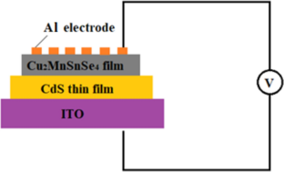
The authors in this work report the formation of high-quality Cu2MnSnSe4 thin films on glass substrates utilizing electron beam deposition. The X-ray diffraction (XRD) investigations of the Cu2MnSnSe4 samples demonstrate that the as-deposited samples are amorphous, while the films that have been annealed at 250 °C reveal a polycrystalline structure with a single tetragonal phase. The EDX spectra of these Cu2MnSnSe4 films clarified their stoichiometric composition. Moreover, various optical parameters have been calculated with the measurement of transmittance and reflectance spectroscopy in the 400–2500 nm range. The optical band gap values of the Cu2MnSnSe4 films were estimated by Tauc's relationship, and they were reduced from 1.71 to 1.47 eV via enlarging the film thickness. The significant impact of thickness on the optical parameters of these Cu2MnSnSe4 films, such as optical conductivity, extinction coefficient, optical dielectric constant, refractive index, and absorption coefficient, was studied. Furthermore, Miller's equations have been used to evaluate the nonlinear optical parameters such as nonlinear refractive index, first and third-order nonlinear optical susceptibility for the Cu2MnSnSe4 samples. The hot-probe approach indicated that the Cu2MnSnSe4 samples have p-type semiconductor behavior. The DC conductivity study of the Cu2MnSnSe4 samples showed that the activation energy values decreased as the film thickness rose from 174 to 459 nm, while the pre-exponential factor values enlarged. On the other hand, the ITO/CdS/Cu2MnSnSe4/Al heterojunction was prepared. This heterojunction device shows a solar conversion efficiency of 4.45%. The results showed that these Cu2MnSnSe4 samples could be used as a new absorber layer in thin-film solar cells.
中文翻译:
p 型 Cu2MnSnSe4 薄膜作为薄膜太阳能电池的新型吸收层的结构、光学、电学和光伏研究
这项工作的作者报告了利用电子束沉积在玻璃基板上形成高质量 Cu 2 MnSnSe 4薄膜。Cu 2 MnSnSe 4样品的 X 射线衍射 (XRD) 研究表明,沉积样品是无定形的,而在 250 °C 下退火的薄膜显示出具有单一四方相的多晶结构。这些 Cu 2 MnSnSe 4薄膜的 EDX 光谱阐明了它们的化学计量组成。此外,通过测量 400-2500 nm 范围内的透射率和反射率光谱,计算了各种光学参数。Cu 2 MnSnSe的光学带隙值通过Tauc关系估计了4层薄膜,通过增加薄膜厚度将它们从1.71降低到1.47 eV。研究了厚度对这些Cu 2 MnSnSe 4薄膜的光学参数的显着影响,例如光学电导率、消光系数、光学介电常数、折射率和吸收系数。此外,米勒方程已用于评估非线性光学参数,例如 Cu 2 MnSnSe 4样品的非线性折射率、一阶和三阶非线性光学磁化率。热探针方法表明 Cu 2 MnSnSe 4样品具有 p 型半导体行为。Cu 2 MnSnSe 4样品的直流电导率研究表明,随着膜厚度从174 nm增加到459 nm,活化能值降低,而指前因子值增大。另一方面,制备ITO/CdS/Cu 2 MnSnSe 4 /Al异质结。这种异质结器件的太阳能转换效率为 4.45%。结果表明,这些Cu 2 MnSnSe 4样品可用作薄膜太阳能电池中的新型吸收层。


 京公网安备 11010802027423号