当前位置:
X-MOL 学术
›
Adv. Mater.
›
论文详情
Our official English website, www.x-mol.net, welcomes your
feedback! (Note: you will need to create a separate account there.)
A Hemispherical Image Sensor Array Fabricated with Organic Photomemory Transistors
Advanced Materials ( IF 27.4 ) Pub Date : 2022-10-25 , DOI: 10.1002/adma.202203541 Yeongin Kim 1 , Chenxin Zhu 1, 2, 3 , Wen-Ya Lee 2 , Anna Smith 4 , Haowen Ma 3 , Xiang Li 3 , Donghee Son 2, 5 , Naoji Matsuhisa 2 , Jaemin Kim 2 , Won-Gyu Bae 2 , Sung Ho Cho 6 , Myung-Gil Kim 2 , Tadanori Kurosawa 2 , Toru Katsumata 7 , John W F To 2 , Jin Young Oh 2, 8 , Seonghyun Paik 1 , Soo Jin Kim 1 , Lihua Jin 2, 9 , Feng Yan 3 , Jeffrey B-H Tok 2 , Zhenan Bao 2
Advanced Materials ( IF 27.4 ) Pub Date : 2022-10-25 , DOI: 10.1002/adma.202203541 Yeongin Kim 1 , Chenxin Zhu 1, 2, 3 , Wen-Ya Lee 2 , Anna Smith 4 , Haowen Ma 3 , Xiang Li 3 , Donghee Son 2, 5 , Naoji Matsuhisa 2 , Jaemin Kim 2 , Won-Gyu Bae 2 , Sung Ho Cho 6 , Myung-Gil Kim 2 , Tadanori Kurosawa 2 , Toru Katsumata 7 , John W F To 2 , Jin Young Oh 2, 8 , Seonghyun Paik 1 , Soo Jin Kim 1 , Lihua Jin 2, 9 , Feng Yan 3 , Jeffrey B-H Tok 2 , Zhenan Bao 2
Affiliation
|
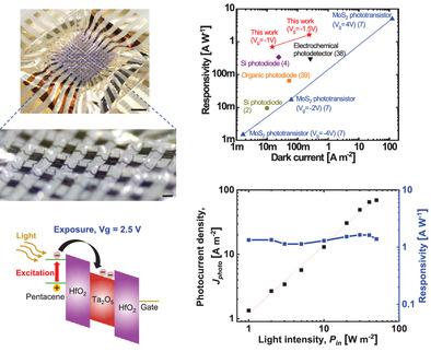
Hemispherical image sensors simplify lens designs, reduce optical aberrations, and improve image resolution for compact wide-field-of-view cameras. To achieve hemispherical image sensors, organic materials are promising candidates due to the following advantages: tunability of optoelectronic/spectral response and low-temperature low-cost processes. Here, a photolithographic process is developed to prepare a hemispherical image sensor array using organic thin film photomemory transistors with a density of 308 pixels per square centimeter. This design includes only one photomemory transistor as a single active pixel, in contrast to the conventional pixel architecture, consisting of select/readout/reset transistors and a photodiode. The organic photomemory transistor, comprising light-sensitive organic semiconductor and charge-trapping dielectric, is able to achieve a linear photoresponse (light intensity range, from 1 to 50 W m−2), along with a responsivity as high as 1.6 A W−1 (wavelength = 465 nm) for a dark current of 0.24 A m−2 (drain voltage = −1.5 V). These observed values represent the best responsivity for similar dark currents among all the reported hemispherical image sensor arrays to date. A transfer method was further developed that does not damage organic materials for hemispherical organic photomemory transistor arrays. These developed techniques are scalable and are amenable for other high-resolution 3D organic semiconductor devices.
中文翻译:

用有机光存储晶体管制造的半球形图像传感器阵列
半球形图像传感器简化了镜头设计,减少了光学像差,并提高了紧凑型宽视场相机的图像分辨率。为了实现半球形图像传感器,有机材料由于以下优点而成为有前途的候选者:光电/光谱响应的可调性和低温低成本工艺。在这里,开发了一种光刻工艺,使用密度为每平方厘米 308 个像素的有机薄膜光存储晶体管制备半球形图像传感器阵列。这种设计仅包括一个光存储晶体管作为单个有源像素,这与传统的像素架构形成鲜明对比,传统像素架构由选择/读出/重置晶体管和光电二极管组成。有机光存储晶体管,包括光敏有机半导体和电荷俘获电介质,−2 ),对于 0.24 A m −2的暗电流(漏极电压 = −1.5 V),响应率高达 1.6 AW −1 (波长 = 465 nm)。这些观测值代表了迄今为止所有报告的半球形图像传感器阵列中类似暗电流的最佳响应率。进一步开发了一种转移方法,该方法不会损坏半球形有机光存储晶体管阵列的有机材料。这些开发的技术具有可扩展性,适用于其他高分辨率 3D 有机半导体设备。
更新日期:2022-10-25
中文翻译:
用有机光存储晶体管制造的半球形图像传感器阵列
半球形图像传感器简化了镜头设计,减少了光学像差,并提高了紧凑型宽视场相机的图像分辨率。为了实现半球形图像传感器,有机材料由于以下优点而成为有前途的候选者:光电/光谱响应的可调性和低温低成本工艺。在这里,开发了一种光刻工艺,使用密度为每平方厘米 308 个像素的有机薄膜光存储晶体管制备半球形图像传感器阵列。这种设计仅包括一个光存储晶体管作为单个有源像素,这与传统的像素架构形成鲜明对比,传统像素架构由选择/读出/重置晶体管和光电二极管组成。有机光存储晶体管,包括光敏有机半导体和电荷俘获电介质,−2 ),对于 0.24 A m −2的暗电流(漏极电压 = −1.5 V),响应率高达 1.6 AW −1 (波长 = 465 nm)。这些观测值代表了迄今为止所有报告的半球形图像传感器阵列中类似暗电流的最佳响应率。进一步开发了一种转移方法,该方法不会损坏半球形有机光存储晶体管阵列的有机材料。这些开发的技术具有可扩展性,适用于其他高分辨率 3D 有机半导体设备。


 京公网安备 11010802027423号