Nano Research ( IF 9.5 ) Pub Date : 2022-10-20 , DOI: 10.1007/s12274-022-4954-6 Lingyao Meng , Ningning Zhang , Maolong Yang , Xixi Yuan , Maliang Liu , Huiyong Hu , Liming Wang
|
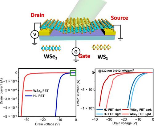
The properties of photodetectors based on two-dimensional materials can be significantly enhanced by avalanche effect. However, a high avalanche breakdown voltage is needed to reach impact ionization, which leads to high power consumption. Here, we report the unique features of a low-voltage avalanche phototransistor formed by an in-plane WSe2 field effect transistor (FET) with an out-of-plane WSe2/WS2 P—N heterojunction (HJ FET). The avalanche breakdown voltage in the device can be decreased from −31 to −8.5 V when compared with that in WSe2 FET. The inherent mechanism is mainly related to the redistributed electric field in the WSe2 channel after the formation of the out-of-plane P—N heterojunction. When the bias voltage is −16.5 V, the photoresponsivity in the HJ FET is enhanced from 1.5 to 135 A/W, which is significantly higher than that in the WSe2 FET because of the obvious reduction of the avalanche breakdown voltage. Moreover, HJ FET shows a higher responsivity than WSe2 FET in the range of 400–1,100 nm under low bias voltage. This phenomenon is caused by accelerating electron—hole spatial separation in the heterojunction. These results indicate that the use of an WSe2 FET with an out-of-plane WSe2/WS2 heterojunction is ideal for high-performance photodetectors with low power consumption.
中文翻译:

具有平面外 WSe2/WS2 异质结的低电压和高增益 WSe2 雪崩光电晶体管
雪崩效应可以显着增强基于二维材料的光电探测器的性能。然而,要达到碰撞电离需要较高的雪崩击穿电压,从而导致高功耗。在这里,我们报告了由平面内 WSe 2场效应晶体管 (FET) 与平面外 WSe 2 /WS 2 PN异质结 (HJ FET)形成的低压雪崩光电晶体管的独特特性。与WSe 2 FET相比,器件中的雪崩击穿电压可以从-31 V 降低到-8.5 V。内在机制主要与WSe 2中的重新分布电场有关面外PN异质结形成后的通道。当偏置电压为-16.5 V时,HJ FET的光响应性从1.5 A/W提高到135 A/W,由于雪崩击穿电压明显降低,明显高于WSe 2 FET。此外,在低偏置电压下,HJ FET 在 400–1,100 nm 范围内显示出比 WSe 2 FET 更高的响应度。这种现象是由加速异质结中的电子-空穴空间分离引起的。这些结果表明,使用具有平面外WSe 2 /WS 2异质结的WSe 2 FET是低功耗高性能光电探测器的理想选择。




















 京公网安备 11010802027423号