Sensors and Actuators A: Physical ( IF 4.1 ) Pub Date : 2022-09-21 , DOI: 10.1016/j.sna.2022.113893 B.S. Ajith Kumar , T. Prakash
|
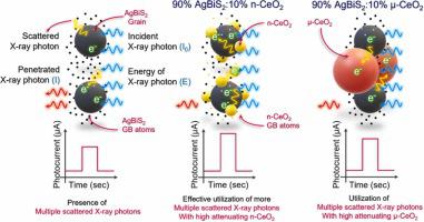
Semiconductor-based direct conversion X-ray sensors have widespread applications spanning from medical diagnosis to industrial inspection. However, current findings on X-ray detection based on perovskites shows high sensitivity but exhibit large leakage current and poor stability, thus, inhibiting them from commercialization. Highly stable AgBiS2 with large attenuation coefficient (μ = 3.07 g cm−2 at 70 keV), shows excellent charge conversion due to its higher atomic number (Bi, Z = 83), and density (ρ = 7.02 g cm−3) was used for X-ray detection. Here, we approach to enhance the net sensitivity of AgBiS2 by tailoring all three parameters by segregating micro/ nanocrystals of cerium oxide (CeO2) at the AgBiS2 grain boundary (GB) region. From the X-ray impinged photocurrent response, substantial GB segregation of n-CeO2 at the AgBiS2 interface leads to improved attenuation and promotes the conversion of multiple scattered X-ray photons into electrons by interacting with the adjacent grains, thus resulting in enhanced photocurrent generation. The sensitivity (S) and noise equivalent dose (NED) ratio were calculated to determine the lowest detectivity of the sensor with less generated noise signals. From these experimental findings, 10 % of n-CeO2 segregation leads to an improvement in the sensitivity of AgBiS2 to 29 μC mGy−1 cm−3.
中文翻译:

基于微/纳米 CeO2 分离 AgBiS2 的 X 射线传感器,用于低剂量检测
基于半导体的直接转换 X 射线传感器具有从医学诊断到工业检测的广泛应用。然而,目前基于钙钛矿的 X 射线检测结果显示出高灵敏度,但泄漏电流大且稳定性差,因此阻碍了它们的商业化。具有大衰减系数(μ = 3.07 g cm -2 at 70 keV)的高度稳定的 AgBiS 2 ,由于其较高的原子序数(Bi,Z = 83)和密度(ρ = 7.02 g cm -3)而显示出优异的电荷转换用于X射线检测。在这里,我们通过在 AgBiS 处分离氧化铈 (CeO 2 ) 的微/纳米晶体来调整所有三个参数来提高 AgBiS 2的净灵敏度。2晶界(GB)区域。从 X 射线撞击光电流响应来看,在 AgBiS 2界面处 n-CeO 2的大量 GB 偏析导致衰减改善,并通过与相邻晶粒相互作用促进多个散射 X 射线光子转化为电子,从而导致增强光电流产生。计算灵敏度 (S) 和噪声当量剂量 (NED) 比率以确定传感器的最低检测率,产生较少的噪声信号。根据这些实验结果,10%的n-CeO 2偏析导致AgBiS 2对29μC mGy -1 cm -3的灵敏度提高。














 京公网安备 11010802027423号