当前位置:
X-MOL 学术
›
ACS Appl. Nano Mater.
›
论文详情
Our official English website, www.x-mol.net, welcomes your
feedback! (Note: you will need to create a separate account there.)
Inheriting Sb2Se3 Nanorods on Sb2S3 Nanorod Arrays for Effective Light Harvesting and Charge Extraction in Solar Cells
ACS Applied Nano Materials ( IF 5.3 ) Pub Date : 2022-08-29 , DOI: 10.1021/acsanm.2c02661
Boyang Zhou 1 , Takaki Kimura 1 , Yutaka Okazaki 1 , Kan Hachiya 1 , Takashi Sagawa 1
ACS Applied Nano Materials ( IF 5.3 ) Pub Date : 2022-08-29 , DOI: 10.1021/acsanm.2c02661
Boyang Zhou 1 , Takaki Kimura 1 , Yutaka Okazaki 1 , Kan Hachiya 1 , Takashi Sagawa 1
Affiliation
|
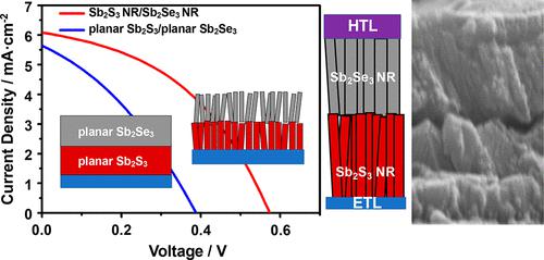
Antimony selenide (Sb2Se3) has great potential as a light-harvesting device in terms of its stability, nontoxicity, and photoelectric properties. Sb2Se3 has a one-dimensional (1D) crystal structure consisting of covalently bonded (Sb4Se6)n ribbons stacking together through van der Waals forces similar to the 1D structure of Sb2S3. This 1D anisotropic structure results in favorable electrical and optical properties for photovoltaics. Many Sb2Se3-based photovoltaic device studies have been focused on the oriental growth of a bulk Sb2Se3 layer. On the contrary, a nanorod array is more preferable for carrier directional transport due to the 1D crystal structure than a bulk thin film compared with a bulk layer. However, few studies have undertaken strategies for the preparation of 1D Sb2Se3 nanorod arrays. In this context, a facile method for the preparation of Sb2Se3 nanorod arrays on a substrate is urgently needed. In this work, we present a solvothermal method that can grow Sb2Se3 nanorods on antimony sulfide (Sb2S3) nanorod arrays enlightened by the advantages of the combination of Sb2S3 and Sb2Se3 such as a light-absorbing layer composed of a Sb2S3 nanorod array/Sb2Se3 nanorod array heterojunction for solar cells. An external quantum efficiency (EQE) at 370 nm of 75% was attained with an optimized device structure of glass-fluorine-doped tin oxide/ZnO/ZnO–ZnS/Sb2S3 nanorod array/Sb2Se3 nanorod array/poly(3-hexylthiophene-2,5-diyl)/MoOx/Ag. This was 2.5 times higher than that of a device using planar Sb2S3/planar Sb2Se3 as a light-absorbing layer. Improvement of the open-circuit voltage from 0.38 V with a planar device to 0.57 V with a nanorod array heterojunction was also confirmed, and a maximum power conversion efficiency of 1.50% was attained with an optimized nanorod array device. This research provides a facile method for the preparation of Sb2Se3 nanorod arrays and a method of combining two layers of inherited Sb2Se3 nanorods on Sb2S3 nanorod arrays compared with the bulk layers of a planar heterojunction, which provides comprehensive information for further optimization of antimony chalcogenide-based photovoltaics.
中文翻译:

在 Sb2S3 纳米棒阵列上继承 Sb2Se3 纳米棒,用于太阳能电池中的有效光捕获和电荷提取
硒化锑(Sb 2 Se 3)在稳定性、无毒性和光电性能方面具有作为光捕获器件的巨大潜力。Sb 2 Se 3具有一维 (1D) 晶体结构,由通过范德华力堆叠在一起的共价键合 (Sb 4 Se 6 ) n带组成,类似于 Sb 2 S 3的一维结构。这种 1D 各向异性结构为光伏器件带来了良好的电学和光学特性。许多基于 Sb 2 Se 3的光伏器件研究都集中在大块 Sb 2的定向生长上Se 3层。相反,与体层相比,由于 1D 晶体结构,纳米棒阵列比体薄膜更适合载流子定向传输。然而,很少有研究采取策略来制备一维 Sb 2 Se 3纳米棒阵列。在此背景下,迫切需要一种简便的方法在基板上制备Sb 2 Se 3纳米棒阵列。在这项工作中,我们提出了一种可以在硫化锑 (Sb 2 S 3 ) 纳米棒阵列上生长 Sb 2 Se 3纳米棒的溶剂热法,该方法受到 Sb 2 S 3组合优势的启发Sb 2 Se 3如太阳能电池用Sb 2 S 3纳米棒阵列/Sb 2 Se 3纳米棒阵列异质结构成的吸光层。采用玻璃-氟掺杂氧化锡/ZnO/ZnO–ZnS/Sb 2 S 3纳米棒阵列/Sb 2 Se 3纳米棒阵列/多晶硅的优化器件结构,在 370 nm 处的外部量子效率 (EQE) 达到 75% (3-己基噻吩-2,5-二基)/MoO x /Ag。这比使用平面 Sb 2 S 3 /平面 Sb 2 Se 3的器件高 2.5 倍作为吸光层。还证实了开路电压从平面器件的 0.38 V 提高到纳米棒阵列异质结的 0.57 V,并且通过优化的纳米棒阵列器件获得了 1.50% 的最大功率转换效率。本研究为制备 Sb 2 Se 3纳米棒阵列提供了一种简便的方法,并提供了一种在 Sb 2 S 3纳米棒阵列上结合两层继承 Sb 2 Se 3纳米棒的方法,与平面异质结的体层相比,提供了全面的进一步优化基于锑硫族化物的光伏发电的信息。
更新日期:2022-08-29
中文翻译:
在 Sb2S3 纳米棒阵列上继承 Sb2Se3 纳米棒,用于太阳能电池中的有效光捕获和电荷提取
硒化锑(Sb 2 Se 3)在稳定性、无毒性和光电性能方面具有作为光捕获器件的巨大潜力。Sb 2 Se 3具有一维 (1D) 晶体结构,由通过范德华力堆叠在一起的共价键合 (Sb 4 Se 6 ) n带组成,类似于 Sb 2 S 3的一维结构。这种 1D 各向异性结构为光伏器件带来了良好的电学和光学特性。许多基于 Sb 2 Se 3的光伏器件研究都集中在大块 Sb 2的定向生长上Se 3层。相反,与体层相比,由于 1D 晶体结构,纳米棒阵列比体薄膜更适合载流子定向传输。然而,很少有研究采取策略来制备一维 Sb 2 Se 3纳米棒阵列。在此背景下,迫切需要一种简便的方法在基板上制备Sb 2 Se 3纳米棒阵列。在这项工作中,我们提出了一种可以在硫化锑 (Sb 2 S 3 ) 纳米棒阵列上生长 Sb 2 Se 3纳米棒的溶剂热法,该方法受到 Sb 2 S 3组合优势的启发Sb 2 Se 3如太阳能电池用Sb 2 S 3纳米棒阵列/Sb 2 Se 3纳米棒阵列异质结构成的吸光层。采用玻璃-氟掺杂氧化锡/ZnO/ZnO–ZnS/Sb 2 S 3纳米棒阵列/Sb 2 Se 3纳米棒阵列/多晶硅的优化器件结构,在 370 nm 处的外部量子效率 (EQE) 达到 75% (3-己基噻吩-2,5-二基)/MoO x /Ag。这比使用平面 Sb 2 S 3 /平面 Sb 2 Se 3的器件高 2.5 倍作为吸光层。还证实了开路电压从平面器件的 0.38 V 提高到纳米棒阵列异质结的 0.57 V,并且通过优化的纳米棒阵列器件获得了 1.50% 的最大功率转换效率。本研究为制备 Sb 2 Se 3纳米棒阵列提供了一种简便的方法,并提供了一种在 Sb 2 S 3纳米棒阵列上结合两层继承 Sb 2 Se 3纳米棒的方法,与平面异质结的体层相比,提供了全面的进一步优化基于锑硫族化物的光伏发电的信息。


 京公网安备 11010802027423号