Journal of Electronic Materials ( IF 2.2 ) Pub Date : 2022-08-17 , DOI: 10.1007/s11664-022-09853-8
M. Njuki , S. Thekkut , R. Das , P. Borgesen , N. Dimitrov
|
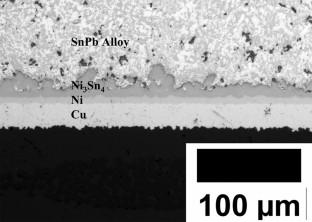
An increasing number of applications of microelectronics products involve multiple reflows and/or extended operation at temperatures high enough that intermetallic growth in the solder joints becomes a concern even on Ni surfaces. Recent work has shown the evolution of large voids between the Ni3Sn4 intermetallic compound and the solder. It was also suggested that the buildup of stresses due to the Kirkendall effect makes this void formation “inevitable” once the Ni3Sn4 thickness has grown to more to more than 5 µm. In a systematic study we find that no voids of any kind are observed in solder joints on high-purity Ni pads, while voiding of different levels of severity is seen upon soldering on electroplated Ni depending on specific processing conditions. We show that while the void growth may result in Ni stress relaxation, the void nucleation is associated with gasification of impurities and/or hydrogen in the Ni during reflow. This is evidenced by the fact that all voiding could be prevented by annealing of electroplated Ni pads to 450°C for 24 h prior to soldering. We argue that, upon nucleation, voids do indeed grow further by coalescence of Kirkendall vacancies created by the disparity of Ni and Sn diffusion fluxes in aging, but the nucleation mechanism renders the voiding propensity controllable and eventually preventable. We discuss the minimization of voiding by control of Ni electroplating and reflow process parameters.
Graphical Abstract
中文翻译:
防止 Ni3Sn4 和焊料之间的空洞生长
越来越多的微电子产品应用涉及多次回流和/或在足够高的温度下延长操作,以至于焊点中的金属间化合物即使在镍表面上也成为一个问题。最近的工作表明,Ni 3 Sn 4金属间化合物和焊料之间会出现大空隙。也有人提出,一旦 Ni 3 Sn 4厚度已增长到超过 5 µm。在一项系统研究中,我们发现在高纯度镍焊盘上的焊点中没有观察到任何类型的空洞,而在电镀镍上焊接时,根据特定的工艺条件,可以看到不同程度的空洞。我们表明,虽然空洞生长可能导致 Ni 应力松弛,但空洞成核与回流期间 Ni 中的杂质和/或氢的气化有关。可以通过在焊接前将电镀镍焊盘退火至 450°C 24 小时来防止所有空洞的事实证明了这一点。我们认为,在成核时,空洞确实会通过老化过程中 Ni 和 Sn 扩散通量的差异产生的 Kirkendall 空位聚结而进一步增长,但成核机制使空洞倾向可控并最终可预防。我们讨论了通过控制镍电镀和回流工艺参数来最小化空洞。


 京公网安备 11010802027423号