当前位置:
X-MOL 学术
›
Small Methods
›
论文详情
Our official English website, www.x-mol.net, welcomes your
feedback! (Note: you will need to create a separate account there.)
Rational Design of WSe2/WS2/WSe2 Dual Junction Phototransistor Incorporating High Responsivity and Detectivity
Small Methods ( IF 10.7 ) Pub Date : 2022-07-24 , DOI: 10.1002/smtd.202200583
Zhongtong Luo 1 , Mengmeng Yang 1 , Dongsi Wu 1 , Zihao Huang 1 , Wei Gao 2 , Menglong Zhang 2 , Yuchen Zhou 1 , Yu Zhao 1 , Zhaoqiang Zheng 1 , Jingbo Li 2, 3
Small Methods ( IF 10.7 ) Pub Date : 2022-07-24 , DOI: 10.1002/smtd.202200583
Zhongtong Luo 1 , Mengmeng Yang 1 , Dongsi Wu 1 , Zihao Huang 1 , Wei Gao 2 , Menglong Zhang 2 , Yuchen Zhou 1 , Yu Zhao 1 , Zhaoqiang Zheng 1 , Jingbo Li 2, 3
Affiliation
|
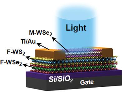
The excellent semiconducting properties and ultrathin morphological characteristics allow van der Waals (vdW) heterostructures based on 2D materials to be promising channel materials for the next-generation optoelectronic devices, especially in photodetectors. Although various 2D heterostructure-based photodetectors have been developed, the unavoidable trade-off between responsivity and detectivity remains a critical issue for these devices. Here, an ingenious phototransistor based on WSe2/WS2/WSe2 dual-vdW heterostructures is constructed, performing both high responsivity and detectivity. In the charge neutrality point (gate voltage of −15 V and bias voltage of 1 V), this device demonstrates a pronounced photosensitivity, accompanying with high detectivity of 1.9 × 10¹⁴ Jones, high responsivity of 35.4 A W−1, and fast rise/fall time of 3.2/2.5 ms at 405 nm with power density of 60 µW cm−2. Density functional theory calculations, energy band profiles, and optoelectronic characteristics jointly verify that the high performance is ascribed to the distinctive device design, which not only facilitates the separation of photogenerated carriers but also produces a strong photogating effect. As a feasible application, an automotive radar system is demonstrated, proving that the device has considerable potential for application in vehicle intelligent assisted driving.
中文翻译:

WSe2/WS2/WSe2高响应度和高检测度双结光电晶体管的合理设计
优异的半导体性能和超薄形态特征使基于二维材料的范德华(vdW)异质结构成为下一代光电器件,特别是光电探测器的有前途的通道材料。尽管已经开发了各种基于 2D 异质结构的光电探测器,但响应度和探测度之间不可避免的权衡仍然是这些设备的关键问题。这里,一个巧妙的基于WSe 2 /WS 2 /WSe 2的光电晶体管构建了双 vdW 异质结构,具有高响应度和检测能力。在电荷中性点(-15 V 的栅极电压和 1 V 的偏置电压),该器件表现出显着的光敏性,伴随着 1.9 × 10 14 Jones 的高检测率、35.4 A W -1的高响应率和快速上升/在 405 nm 处的下降时间为 3.2/2.5 ms,功率密度为 60 µW cm -2. 密度泛函理论计算、能带分布和光电特性共同验证了高性能归因于独特的器件设计,不仅有利于光生载流子的分离,而且产生了强大的光选通效应。作为一个可行的应用,汽车雷达系统被演示,证明该设备在汽车智能辅助驾驶中具有相当大的应用潜力。
更新日期:2022-07-24
中文翻译:
WSe2/WS2/WSe2高响应度和高检测度双结光电晶体管的合理设计
优异的半导体性能和超薄形态特征使基于二维材料的范德华(vdW)异质结构成为下一代光电器件,特别是光电探测器的有前途的通道材料。尽管已经开发了各种基于 2D 异质结构的光电探测器,但响应度和探测度之间不可避免的权衡仍然是这些设备的关键问题。这里,一个巧妙的基于WSe 2 /WS 2 /WSe 2的光电晶体管构建了双 vdW 异质结构,具有高响应度和检测能力。在电荷中性点(-15 V 的栅极电压和 1 V 的偏置电压),该器件表现出显着的光敏性,伴随着 1.9 × 10 14 Jones 的高检测率、35.4 A W -1的高响应率和快速上升/在 405 nm 处的下降时间为 3.2/2.5 ms,功率密度为 60 µW cm -2. 密度泛函理论计算、能带分布和光电特性共同验证了高性能归因于独特的器件设计,不仅有利于光生载流子的分离,而且产生了强大的光选通效应。作为一个可行的应用,汽车雷达系统被演示,证明该设备在汽车智能辅助驾驶中具有相当大的应用潜力。


 京公网安备 11010802027423号