当前位置:
X-MOL 学术
›
Adv. Mater. Technol.
›
论文详情
Our official English website, www.x-mol.net, welcomes your
feedback! (Note: you will need to create a separate account there.)
Room-Temperature Printing of Ultrathin Quasi-2D GaN Semiconductor via Liquid Metal Gallium Surface Confined Nitridation Reaction
Advanced Materials Technologies ( IF 6.4 ) Pub Date : 2022-07-01 , DOI: 10.1002/admt.202200733 Qian Li 1 , Bang‐Deng Du 1 , Jian‐Ye Gao 1, 2 , Bao‐Yu Xing 3 , Dian‐Kai Wang 3 , Ji‐Fei Ye 3 , Jing Liu 1, 4
Advanced Materials Technologies ( IF 6.4 ) Pub Date : 2022-07-01 , DOI: 10.1002/admt.202200733 Qian Li 1 , Bang‐Deng Du 1 , Jian‐Ye Gao 1, 2 , Bao‐Yu Xing 3 , Dian‐Kai Wang 3 , Ji‐Fei Ye 3 , Jing Liu 1, 4
Affiliation
|
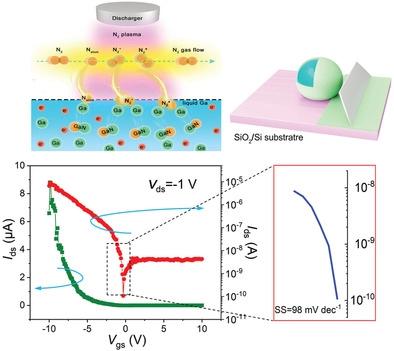
Outstanding wide-bandgap semiconductor material such as gallium nitride (GaN) has been extensively utilized in power electronics, radiofrequency amplifiers, and harsh environment devices. Due to its quantum confinement effect in enabling desired deep-ultraviolet emission, excitonic impact, and electronic transport features, 2D or ultrathin quasi-2D GaN semiconductors have been one of the most remarkable candidates for future growth of microelectronic devices. Here, for the first time, the authors report a large area, wide bandgap, and room-temperature quasi-2D GaN synthesis and printing strategy through introducing the plasma medicated liquid metal gallium surface-confined nitridation reaction mechanism. The developed direct fabrication and compositional process is consistent with various electronics manufacturing approaches and thus opens an easy going way for cost-effective growth of the third-generation semiconductor. In particular, the fully printed field-effect transistors relying on the GaN thus made show p-type switching with an on/off ratio greater than 105, maximum field-effect hole mobility of 53 cm2 V−1 s−1, and a small sub-threshold swing. As demonstrated, the present method allows to produce at room temperature the GaN with thickness spanning from 1 nanometer to nanometers. This basic method can be further extended, generalized, and utilized for making various electronic and photoelectronic devices in the coming time.
中文翻译:

通过液态金属镓表面限制氮化反应的超薄准二维 GaN 半导体的室温印刷
氮化镓 (GaN) 等出色的宽禁带半导体材料已广泛应用于电力电子、射频放大器和恶劣环境设备中。由于其在实现所需的深紫外发射、激子冲击和电子传输特性方面的量子限制效应,二维或超薄准二维 GaN 半导体已成为微电子器件未来增长的最显着候选者之一。在这里,作者首次通过引入等离子体介导的液态金属镓表面约束氮化反应机理,报道了大面积、宽带隙和室温准二维 GaN 的合成和印刷策略。开发的直接制造和组合工艺与各种电子制造方法一致,因此为第三代半导体的成本效益增长开辟了一条简单的道路。特别是,依赖于 GaN 的完全印刷的场效应晶体管显示出 p 型开关,开/关比大于 10如图5所示,最大场效应空穴迁移率为53 cm 2 V -1 s -1,以及小的亚阈值摆动。如所证明的,本方法允许在室温下生产厚度从1纳米到纳米的GaN。这种基本方法可以进一步扩展、推广,并在未来用于制造各种电子和光电器件。
更新日期:2022-07-01
中文翻译:
通过液态金属镓表面限制氮化反应的超薄准二维 GaN 半导体的室温印刷
氮化镓 (GaN) 等出色的宽禁带半导体材料已广泛应用于电力电子、射频放大器和恶劣环境设备中。由于其在实现所需的深紫外发射、激子冲击和电子传输特性方面的量子限制效应,二维或超薄准二维 GaN 半导体已成为微电子器件未来增长的最显着候选者之一。在这里,作者首次通过引入等离子体介导的液态金属镓表面约束氮化反应机理,报道了大面积、宽带隙和室温准二维 GaN 的合成和印刷策略。开发的直接制造和组合工艺与各种电子制造方法一致,因此为第三代半导体的成本效益增长开辟了一条简单的道路。特别是,依赖于 GaN 的完全印刷的场效应晶体管显示出 p 型开关,开/关比大于 10如图5所示,最大场效应空穴迁移率为53 cm 2 V -1 s -1,以及小的亚阈值摆动。如所证明的,本方法允许在室温下生产厚度从1纳米到纳米的GaN。这种基本方法可以进一步扩展、推广,并在未来用于制造各种电子和光电器件。


 京公网安备 11010802027423号