当前位置:
X-MOL 学术
›
J. Mater. Chem. A
›
论文详情
Our official English website, www.x-mol.net, welcomes your
feedback! (Note: you will need to create a separate account there.)
A lateral built-in field of the 2D/2D SnS2/SnSe2 in-plane heterostructure with boosted interfacial charge transfer
Journal of Materials Chemistry A ( IF 10.7 ) Pub Date : 2022-06-20 , DOI: 10.1039/d2ta03333j
Ruozhen Wu 1 , Tiezhu Xin 1 , You Wang 1 , Tingting Wang 1 , Lizhao Liu 2 , Juanyuan Hao 1
Journal of Materials Chemistry A ( IF 10.7 ) Pub Date : 2022-06-20 , DOI: 10.1039/d2ta03333j
Ruozhen Wu 1 , Tiezhu Xin 1 , You Wang 1 , Tingting Wang 1 , Lizhao Liu 2 , Juanyuan Hao 1
Affiliation
|
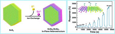
Heterostructure construction is an effective strategy for enhancing the properties of functional materials. However, the problems of lattice mismatch and weak built-in field in the heterointerface usually degrade the interfacial charge transfer efficiency, severely limiting the improvement of sensing properties for gas sensors. To break through this limitation, we attempted to build a lattice-matched SnS2/SnSe2 in-plane heterostructure as a NO2 gas sensor, for which the capability was revealed by DFT calculations. The SnS2/SnSe2 in-plane heterostructures with atomically sharp interfaces were synthesized by the topotactic anion-exchange method. The content and spatial arrangement of in situ grown SnSe2 can be tuned in the heterostructures by adjusting the Se precursor. Ultrahigh response (1165.2%), sensitivity (322.0% ppm−1) and rapid response/recovery (80/78 s) to NO2 (4 ppm) were realized at room temperature for the optimal SnS2/SnSe2 in-plane heterostructure. The response value was 24.7 and 9.5 times higher than that of the common SnS2/SnSe2 heterostructures prepared by mechanical mixing and solvothermal deposition, respectively. The response and recovery times were also improved by a factor of 3.5/8.9 and 1.6/4.9, respectively. The superior sensing properties are attributed to the atomic-level sharp in-plane SnS2/SnSe2 heterointerface with a lateral built-in field that not only improves NO2 adsorption but also boosts the interfacial charge transfer along the 2D plane. The ion-exchange growth of the 2D in-plane heterostructure is expected to expand to other 2D nanomaterial systems for applications in sensors, photoelectronics, and catalysts.
中文翻译:

具有增强的界面电荷转移的 2D/2D SnS2/SnSe2 面内异质结构的横向内建场
异质结构构建是增强功能材料性能的有效策略。然而,异质界面中晶格失配和内建场弱的问题通常会降低界面电荷转移效率,严重限制了气体传感器传感性能的提高。为了突破这一限制,我们尝试构建晶格匹配的 SnS 2 /SnSe 2面内异质结构作为 NO 2气体传感器,其性能通过 DFT 计算得到揭示。通过拓扑阴离子交换法合成了具有原子尖锐界面的SnS 2 /SnSe 2面内异质结构。原地的内容和空间安排生长的 SnSe 2可以通过调整 Se 前体来调整异质结构。在室温下实现了对 NO 2 (4 ppm) 的超高响应 (1165.2%)、灵敏度 (322.0% ppm -1 ) 和快速响应/恢复 (80/78 s),以获得最佳 SnS 2 /SnSe 2面内异质结构. 响应值分别是机械混合和溶剂热沉积制备的普通SnS 2 /SnSe 2异质结构的24.7倍和9.5倍。响应和恢复时间也分别提高了 3.5/8.9 和 1.6/4.9 倍。优异的传感特性归因于原子级尖锐的面内 SnS 2/SnSe 2异质界面具有横向内置场,不仅可以改善 NO 2吸附,还可以促进沿二维平面的界面电荷转移。二维面内异质结构的离子交换生长有望扩展到其他二维纳米材料系统,用于传感器、光电子学和催化剂。
更新日期:2022-06-20
中文翻译:
具有增强的界面电荷转移的 2D/2D SnS2/SnSe2 面内异质结构的横向内建场
异质结构构建是增强功能材料性能的有效策略。然而,异质界面中晶格失配和内建场弱的问题通常会降低界面电荷转移效率,严重限制了气体传感器传感性能的提高。为了突破这一限制,我们尝试构建晶格匹配的 SnS 2 /SnSe 2面内异质结构作为 NO 2气体传感器,其性能通过 DFT 计算得到揭示。通过拓扑阴离子交换法合成了具有原子尖锐界面的SnS 2 /SnSe 2面内异质结构。原地的内容和空间安排生长的 SnSe 2可以通过调整 Se 前体来调整异质结构。在室温下实现了对 NO 2 (4 ppm) 的超高响应 (1165.2%)、灵敏度 (322.0% ppm -1 ) 和快速响应/恢复 (80/78 s),以获得最佳 SnS 2 /SnSe 2面内异质结构. 响应值分别是机械混合和溶剂热沉积制备的普通SnS 2 /SnSe 2异质结构的24.7倍和9.5倍。响应和恢复时间也分别提高了 3.5/8.9 和 1.6/4.9 倍。优异的传感特性归因于原子级尖锐的面内 SnS 2/SnSe 2异质界面具有横向内置场,不仅可以改善 NO 2吸附,还可以促进沿二维平面的界面电荷转移。二维面内异质结构的离子交换生长有望扩展到其他二维纳米材料系统,用于传感器、光电子学和催化剂。


 京公网安备 11010802027423号