当前位置:
X-MOL 学术
›
Appl. Surf. Sci.
›
论文详情
Our official English website, www.x-mol.net, welcomes your
feedback! (Note: you will need to create a separate account there.)
C-Si interface on SiO2/(1 1 1) diamond p-MOSFETs with high mobility and excellent normally-off operation
Applied Surface Science ( IF 6.3 ) Pub Date : 2022-04-11 , DOI: 10.1016/j.apsusc.2022.153368
Xiaohua Zhu 1, 2 , Te Bi 1 , Xiaolu Yuan 2 , Yuhao Chang 1 , Runming Zhang 1 , Yu Fu 1 , Juping Tu 2 , Yabo Huang 2 , Jinlong Liu 2 , Chengming Li 2 , Hiroshi Kawarada 1, 3
Applied Surface Science ( IF 6.3 ) Pub Date : 2022-04-11 , DOI: 10.1016/j.apsusc.2022.153368
Xiaohua Zhu 1, 2 , Te Bi 1 , Xiaolu Yuan 2 , Yuhao Chang 1 , Runming Zhang 1 , Yu Fu 1 , Juping Tu 2 , Yabo Huang 2 , Jinlong Liu 2 , Chengming Li 2 , Hiroshi Kawarada 1, 3
Affiliation
|
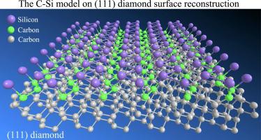
In this paper, a diamond-silicon (C-Si) interface was constructed on a (12 gate insulator in a reductive atmosphere. Corresponding metal-oxide-semiconductor field effect transistors (MOSFETs) with a C-Si conductive channel were fabricated. The MOSFETs demonstrate excellent normally-off operation with a high threshold voltage (V th ) of −16 V and a high current density of −167 mA/mm, with a gate length (L G ) of 4 μm. The channel hole mobility (μ FE ) reaches 200 cm2 V−1 s−1 with a L G of 10 μm, and the interface state density (D it ) is as low as 3.8 × 1011 cm−2 eV−1 . The high-resolution transmission electron microscopy (HRTEM) image displays a coherent and strain-free interface between the SiO2 film and (1μ FE and low D it in the MOSFETs. The interface is dominated by C-Si bonds, which are confirmed by atomic-scale electron energy loss (EELS) quantification, spectroscopic characterization, and X-ray photoelectron spectroscopy (XPS). These results demonstrate that diamond, directly combined with SiO2 , is ideal for implementation in power devices.
中文翻译:

SiO2/(1 1 1) 金刚石 p-MOSFET 上的 C-Si 接口具有高迁移率和出色的常闭操作
在本文中,通过在还原气氛中退火 SiO2 栅极绝缘体,在 (111) 金刚石衬底上构建了金刚石-硅 (C-Si) 界面。制造了相应的具有 C-Si 导电通道的金属氧化物半导体场效应晶体管 (MOSFET)。MOSFET 表现出优异的常闭操作性能,具有 −16 V 的高阈值电压 (Vth) 和 −167 mA/mm 的高电流密度,栅极长度 (LG) 为 4 μm。通道空穴迁移率 (μFE) 达到 200 cm2V-1s-1,LG 为 10 μm,界面状态密度 (Dit) 低至 3.8 × 1011 cm-2 eV-1。高分辨率透射电子显微镜 (HRTEM) 图像显示了 SiO2 薄膜和 (111) 金刚石之间的连贯且无应变的界面,从而确保了 MOSFET 中的高 μFE 和低 Dit。界面以 C-Si 键为主,原子级电子能量损失 (EELS) 量化、光谱表征和 X 射线光电子能谱 (XPS) 证实了这一点。这些结果表明,金刚石与 SiO2 直接结合,非常适合在功率器件中实现。
更新日期:2022-04-11
中文翻译:
SiO2/(1 1 1) 金刚石 p-MOSFET 上的 C-Si 接口具有高迁移率和出色的常闭操作
在本文中,通过在还原气氛中退火 SiO2 栅极绝缘体,在 (111) 金刚石衬底上构建了金刚石-硅 (C-Si) 界面。制造了相应的具有 C-Si 导电通道的金属氧化物半导体场效应晶体管 (MOSFET)。MOSFET 表现出优异的常闭操作性能,具有 −16 V 的高阈值电压 (Vth) 和 −167 mA/mm 的高电流密度,栅极长度 (LG) 为 4 μm。通道空穴迁移率 (μFE) 达到 200 cm2V-1s-1,LG 为 10 μm,界面状态密度 (Dit) 低至 3.8 × 1011 cm-2 eV-1。高分辨率透射电子显微镜 (HRTEM) 图像显示了 SiO2 薄膜和 (111) 金刚石之间的连贯且无应变的界面,从而确保了 MOSFET 中的高 μFE 和低 Dit。界面以 C-Si 键为主,原子级电子能量损失 (EELS) 量化、光谱表征和 X 射线光电子能谱 (XPS) 证实了这一点。这些结果表明,金刚石与 SiO2 直接结合,非常适合在功率器件中实现。


 京公网安备 11010802027423号