Journal of Sol-Gel Science and Technology ( IF 2.3 ) Pub Date : 2022-01-09 , DOI: 10.1007/s10971-021-05683-y A. Panneerselvam 1 , K. S. Mohan 2 , R. Marnadu 3 , J. Chandrasekaran 3
|
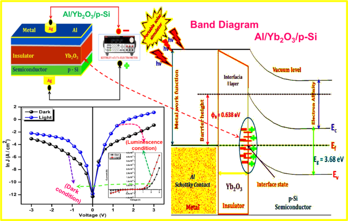
The present research explores the fabrication of a metal insulator semiconductor Schottky barrier diode (SBD) with rare earth metal oxide (Yb2O3) thin films as insulators that are effectively developed on a large scale using the low-cost jet nebulizer spray pyrolysis technique (JNSP). The Yb2O3 thin films are deposited at various substrate temperatures (350 °C–550 °C) to ascertain its influence on the characteristic properties of the material. The structural, morphological and opto-electrical properties are investigated using various characterization techniques. Here, X-ray diffraction (XRD) analysis revealed the single crystalline cubic crystal structure of Yb2O3 thin films. Field emission scanning electron microscope (FESEM) images show the presence of uniformly distributed cage and globular like structures spread over the entire surface of the Yb2O3 films. The elemental composition study demonstrates the presence of Yb and O. The optical direct energy band gap of Yb2O3 thin films have been analyzed through UV-Visible spectra. Current – voltage measurements were analyzed in dark and light conditions for the Al/Yb2O3/p-Si structured Schottky barrier diodes (SBDs) which are fabricated with interfacial layers at different substrate temperatures. Further, the functionality of the SBDs was tested at different temperatures ranging from 30 °C to 150 °C. The experimental results of all SBDs indicate a linear reduction in the ideality factor (n) up to 2.537 and 2.059 with a slight increase in the effective barrier height (ФB) of 0.789 eV& 0.638 in dark and light conditions, respectively. The SBD fabricated at 550 °C recorded good performance, which will be suitable for thermal dependent electronic device applications.
中文翻译:
Yb2O3薄膜结构和光电性能的深入研究以及Al/Yb2O3/p-Si (MIS)肖特基势垒二极管的制备
本研究探索了一种金属绝缘体半导体肖特基势垒二极管 (SBD) 的制造,其中稀土金属氧化物 (Yb 2 O 3 ) 薄膜作为绝缘体,使用低成本喷射雾化器喷雾热解技术可大规模有效地开发。 (JNSP)。Yb 2 O 3薄膜在不同的衬底温度(350°C-550°C)下沉积,以确定其对材料特性的影响。使用各种表征技术研究结构、形态和光电特性。在这里,X射线衍射(XRD)分析揭示了Yb 2 O 3 的单晶立方晶体结构薄膜。场发射扫描电子显微镜 (FESEM) 图像显示存在分布在 Yb 2 O 3薄膜的整个表面上的均匀分布的笼和球状结构。元素组成研究表明存在 Yb 和 O。通过紫外-可见光谱分析了 Yb 2 O 3薄膜的光学直接能带隙。在黑暗和光照条件下分析了 Al/Yb 2 O 3 的电流 - 电压测量值/p-Si 结构的肖特基势垒二极管 (SBD),在不同衬底温度下用界面层制造。此外,SBD 的功能在 30 °C 至 150 °C 的不同温度下进行了测试。所有 SBD 的实验结果表明,理想因子 ( n )线性降低至 2.537 和 2.059,有效势垒高度 (Ф B ) 在黑暗和光照条件下分别略有增加0.789 eV 和 0.638。在 550 °C 下制造的 SBD 记录了良好的性能,这将适用于热相关的电子设备应用。


 京公网安备 11010802027423号