当前位置:
X-MOL 学术
›
ACS Appl. Electron. Mater.
›
论文详情
Our official English website, www.x-mol.net, welcomes your
feedback! (Note: you will need to create a separate account there.)
Split-Gate Photodiode Based on Graphene/HgTe Heterostructures with a Few Nanosecond Photoresponse
ACS Applied Electronic Materials ( IF 4.3 ) Pub Date : 2021-11-04 , DOI: 10.1021/acsaelm.1c00442 Charlie Gréboval 1 , Corentin Dabard 1, 2 , Nikita Konstantinov 3 , Mariarosa Cavallo 1 , Sang-Soo Chee 1 , Audrey Chu 1 , Tung Huu Dang 1 , Adrien Khalili 1 , Eva Izquierdo 1 , Yoann Prado 1 , Hicham Majjad 3 , Xiang Zhen Xu 2 , Jean-Francois Dayen 3, 4 , Emmanuel Lhuillier 1
ACS Applied Electronic Materials ( IF 4.3 ) Pub Date : 2021-11-04 , DOI: 10.1021/acsaelm.1c00442 Charlie Gréboval 1 , Corentin Dabard 1, 2 , Nikita Konstantinov 3 , Mariarosa Cavallo 1 , Sang-Soo Chee 1 , Audrey Chu 1 , Tung Huu Dang 1 , Adrien Khalili 1 , Eva Izquierdo 1 , Yoann Prado 1 , Hicham Majjad 3 , Xiang Zhen Xu 2 , Jean-Francois Dayen 3, 4 , Emmanuel Lhuillier 1
Affiliation
|
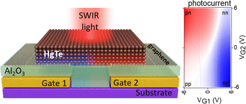
Hopping transport associated with the granular nature of nanocrystal arrays has led to the thought that nanocrystal-based devices might be incompatible with fast operation. Here, we explore the design of HgTe nanocrystal-based sensors operating in the short-wave infrared and with a very fast time response down to a few nanoseconds. To reach this goal, the design relies on a planar geometry to reduce the device capacitance. A strong in-built electric field is tailored via electrostatic control from two bottom split-gate electrodes, which promote the charge extraction. Through the use of graphene electrodes patterned over the two gate electrodes, we optimize the control on the electrostatic design of the p–n junction inside the nanocrystal array. Taking advantage of a high-k dielectric spacer, we demonstrate that the device can be operated under a low gate bias (<6 V). The split-gate photodetector are versatile as they can be used in either the phototransistor or diode mode, with the two gates voltages that are set to design isotype or diode-type heterojunctions. We finally highlight that the time response enabled by the planar diode configuration can be made much faster than the one associated with the conventional vertical geometry.
中文翻译:

基于具有几纳秒光响应的石墨烯/HgTe异质结构的分裂栅光电二极管
与纳米晶体阵列的颗粒性质相关的跳跃传输导致人们认为基于纳米晶体的设备可能与快速操作不兼容。在这里,我们探索了基于 HgTe 纳米晶体的传感器的设计,该传感器在短波红外线下工作,并且具有低至几纳秒的非常快的时间响应。为了达到这个目标,该设计依赖于平面几何结构来降低器件电容。通过来自两个底部分裂栅电极的静电控制来定制强大的内置电场,从而促进电荷提取。通过使用在两个栅电极上图案化的石墨烯电极,我们优化了对纳米晶体阵列内部 p-n 结静电设计的控制。利用高k介电隔离物,我们证明该器件可以在低栅极偏压(<6 V)下运行。分裂栅光电探测器是通用的,因为它们可用于光电晶体管或二极管模式,两个栅极电压设置为设计同型或二极管型异质结。我们最后强调,由平面二极管配置实现的时间响应可以比与传统垂直几何结构相关的时间响应快得多。
更新日期:2021-11-23
中文翻译:
基于具有几纳秒光响应的石墨烯/HgTe异质结构的分裂栅光电二极管
与纳米晶体阵列的颗粒性质相关的跳跃传输导致人们认为基于纳米晶体的设备可能与快速操作不兼容。在这里,我们探索了基于 HgTe 纳米晶体的传感器的设计,该传感器在短波红外线下工作,并且具有低至几纳秒的非常快的时间响应。为了达到这个目标,该设计依赖于平面几何结构来降低器件电容。通过来自两个底部分裂栅电极的静电控制来定制强大的内置电场,从而促进电荷提取。通过使用在两个栅电极上图案化的石墨烯电极,我们优化了对纳米晶体阵列内部 p-n 结静电设计的控制。利用高k介电隔离物,我们证明该器件可以在低栅极偏压(<6 V)下运行。分裂栅光电探测器是通用的,因为它们可用于光电晶体管或二极管模式,两个栅极电压设置为设计同型或二极管型异质结。我们最后强调,由平面二极管配置实现的时间响应可以比与传统垂直几何结构相关的时间响应快得多。


 京公网安备 11010802027423号