当前位置:
X-MOL 学术
›
Adv. Mater.
›
论文详情
Our official English website, www.x-mol.net, welcomes your
feedback! (Note: you will need to create a separate account there.)
Organic Semiconductor Crystal Engineering for High-Resolution Layer-Controlled 2D Crystal Arrays
Advanced Materials ( IF 27.4 ) Pub Date : 2021-08-20 , DOI: 10.1002/adma.202104166
Zheng Chen 1 , Shuming Duan 1, 2 , Xiaotao Zhang 3 , Bowen Geng 1 , Yanling Xiao 4 , Jiansheng Jie 4 , Huanli Dong 5 , Liqiang Li 3 , Wenping Hu 1, 2
Advanced Materials ( IF 27.4 ) Pub Date : 2021-08-20 , DOI: 10.1002/adma.202104166
Zheng Chen 1 , Shuming Duan 1, 2 , Xiaotao Zhang 3 , Bowen Geng 1 , Yanling Xiao 4 , Jiansheng Jie 4 , Huanli Dong 5 , Liqiang Li 3 , Wenping Hu 1, 2
Affiliation
|
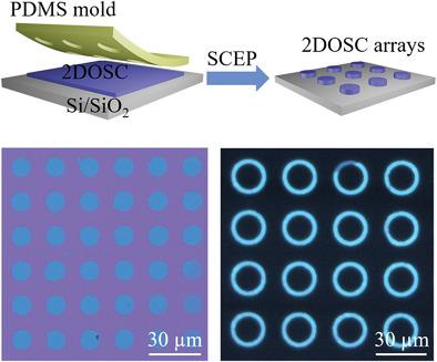
2D organic semiconductor crystals (2DOSCs) have extraordinary charge transport capability, adjustable photoelectric properties, and superior flexibility, and have stimulated continuous research interest for next-generation electronic and optoelectronic applications. The prerequisite for achieving large-area and high-throughput optoelectronic device integration is to fabricate high-resolution 2DOSC arrays. Patterned substrate- and template-assisted self-assembly is an effective strategy to fabricate OSC arrays. However, the film thickness is difficult to control due to the complicated crystallization process during solvent evaporation. Therefore, the manufacturing of 2DOSC arrays with high-resolution and controllable molecular-layer numbers through solution-based patterning methods remains a challenge. Herein, a two-step strategy to produce high-resolution layer-controlled 2DOSC arrays is reported. First, large-scale 2DOSCs with well-defined layer numbers are obtained by a solution-processed organic semiconductor crystal engineering method. Next, the high-resolution layer-controlled 2DOSC arrays are fabricated by a polydimethylsiloxane mold-assisted selective contact evaporation printing technique. The organic field-effect transistors (OFETs) based on 2DOSC arrays have high electrical performance and excellent uniformity. The 2,6-bis(4-hexylphenyl)anthracene 2DOSC arrays-based OFETs have a small variation of 12.5% in mobility. This strategy can be applied to various organic semiconductors and pattern arrays. These demonstrations will offer more opportunities for 2DOSCs for integrated optoelectronic devices.
中文翻译:

用于高分辨率层控制二维晶体阵列的有机半导体晶体工程
二维有机半导体晶体(2DOSCs)具有非凡的电荷传输能力、可调节的光电特性和卓越的柔韧性,激发了对下一代电子和光电应用的持续研究兴趣。实现大面积、高通量光电器件集成的先决条件是制作高分辨率的2DOSC阵列。图案化基板和模板辅助自组装是制造 OSC 阵列的有效策略。然而,由于溶剂蒸发过程中复杂的结晶过程,薄膜厚度难以控制。因此,通过基于溶液的图案化方法制造具有高分辨率和可控分子层数的 2DOSC 阵列仍然是一个挑战。在此处,报告了生产高分辨率层控制 2DOSC 阵列的两步策略。首先,通过溶液处理有机半导体晶体工程方法获得具有明确层数的大规模2DOSC。接下来,通过聚二甲基硅氧烷模具辅助选择性接触蒸发印刷技术制造高分辨率层控 2DOSC 阵列。基于 2DOSC 阵列的有机场效应晶体管 (OFET) 具有较高的电性能和优异的均匀性。基于 2,6-双(4-己基苯基)蒽 2DOSC 阵列的 OFET 的迁移率变化很小,为 12.5%。该策略可应用于各种有机半导体和图案阵列。这些演示将为集成光电器件的 2DOSC 提供更多机会。
更新日期:2021-08-20
中文翻译:
用于高分辨率层控制二维晶体阵列的有机半导体晶体工程
二维有机半导体晶体(2DOSCs)具有非凡的电荷传输能力、可调节的光电特性和卓越的柔韧性,激发了对下一代电子和光电应用的持续研究兴趣。实现大面积、高通量光电器件集成的先决条件是制作高分辨率的2DOSC阵列。图案化基板和模板辅助自组装是制造 OSC 阵列的有效策略。然而,由于溶剂蒸发过程中复杂的结晶过程,薄膜厚度难以控制。因此,通过基于溶液的图案化方法制造具有高分辨率和可控分子层数的 2DOSC 阵列仍然是一个挑战。在此处,报告了生产高分辨率层控制 2DOSC 阵列的两步策略。首先,通过溶液处理有机半导体晶体工程方法获得具有明确层数的大规模2DOSC。接下来,通过聚二甲基硅氧烷模具辅助选择性接触蒸发印刷技术制造高分辨率层控 2DOSC 阵列。基于 2DOSC 阵列的有机场效应晶体管 (OFET) 具有较高的电性能和优异的均匀性。基于 2,6-双(4-己基苯基)蒽 2DOSC 阵列的 OFET 的迁移率变化很小,为 12.5%。该策略可应用于各种有机半导体和图案阵列。这些演示将为集成光电器件的 2DOSC 提供更多机会。


 京公网安备 11010802027423号