当前位置:
X-MOL 学术
›
ACS Appl. Electron. Mater.
›
论文详情
Our official English website, www.x-mol.net, welcomes your
feedback! (Note: you will need to create a separate account there.)
On the Contact Optimization of ALD-Based MoS2 FETs: Correlation of Processing Conditions and Interface Chemistry with Device Electrical Performance
ACS Applied Electronic Materials ( IF 4.3 ) Pub Date : 2021-06-28 , DOI: 10.1021/acsaelm.1c00379 Reyhaneh Mahlouji 1 , Yue Zhang 2 , Marcel A Verheijen 1, 3 , Jan P Hofmann 2, 4 , Wilhelmus M M Kessels 1 , Abhay A Sagade 5 , Ageeth A Bol 1
ACS Applied Electronic Materials ( IF 4.3 ) Pub Date : 2021-06-28 , DOI: 10.1021/acsaelm.1c00379 Reyhaneh Mahlouji 1 , Yue Zhang 2 , Marcel A Verheijen 1, 3 , Jan P Hofmann 2, 4 , Wilhelmus M M Kessels 1 , Abhay A Sagade 5 , Ageeth A Bol 1
Affiliation
|
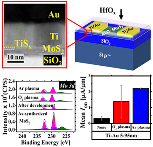
Despite the extensive ongoing research on MoS2 field effect transistors (FETs), the key role of device processing conditions in the chemistry involved at the metal-to-MoS2 interface and their influence on the electrical performance are often overlooked. In addition, the majority of reports on MoS2 contacts are based on exfoliated MoS2, whereas synthetic films are even more susceptible to the changes made in device processing conditions. In this paper, working FETs with atomic layer deposition (ALD)-based MoS2 films and Ti/Au contacts are demonstrated, using current–voltage (I–V) characterization. In pursuit of optimizing the contacts, high-vacuum thermal annealing as well as O2/Ar plasma cleaning treatments are introduced, and their influence on the electrical performance is studied. The electrical findings are linked to the interface chemistry through X-ray photoelectron spectroscopy (XPS) and scanning transmission electron microscopy (STEM) analyses. XPS evaluation reveals that the concentration of organic residues on the MoS2 surface, as a result of resist usage during the device processing, is significant. Removal of these contaminations with O2/Ar plasma changes the MoS2 chemical state and enhances the MoS2 electrical properties. Based on the STEM analysis, the observed progress in the device electrical characteristics could also be associated with the formation of a continuous TiSx layer at the Ti-to-MoS2 interface. Scaling down the Ti interlayer thickness and replacing it with Cr is found to be beneficial as well, leading to further device performance advancements. Our findings are of value for attaining optimal contacts to synthetic MoS2 films.
中文翻译:

基于 ALD 的 MoS2 FET 的接触优化:加工条件和界面化学与器件电性能的相关性
尽管对 MoS 2场效应晶体管 (FET)进行了广泛的研究,但器件加工条件在金属-MoS 2界面所涉及的化学中的关键作用及其对电性能的影响经常被忽视。此外,大多数关于 MoS 2接触的报告都是基于剥离的 MoS 2,而合成薄膜甚至更容易受到器件加工条件变化的影响。在本文中,用原子层沉积工作的FET(ALD)基的MoS 2层膜和Ti / Au的触点证实的,使用电流-电压(我- V) 表征。为了优化接触,引入了高真空热退火和O 2 /Ar等离子体清洗处理,并研究了它们对电气性能的影响。电学发现通过 X 射线光电子能谱 (XPS) 和扫描透射电子显微镜 (STEM) 分析与界面化学相关联。XPS 评估表明,由于在器件加工过程中使用抗蚀剂,MoS 2表面上有机残留物的浓度很重要。用 O 2 /Ar 等离子体去除这些污染物会改变 MoS 2 的化学状态并增强 MoS 2电气特性。基于 STEM 分析,观察到的器件电气特性的进展也可能与Ti-to-MoS 2界面处连续 TiS x层的形成有关。发现按比例缩小 Ti 夹层厚度并用 Cr 代替它也是有益的,从而进一步提高器件性能。我们的发现对于实现与合成 MoS 2薄膜的最佳接触很有价值。
更新日期:2021-07-27
中文翻译:
基于 ALD 的 MoS2 FET 的接触优化:加工条件和界面化学与器件电性能的相关性
尽管对 MoS 2场效应晶体管 (FET)进行了广泛的研究,但器件加工条件在金属-MoS 2界面所涉及的化学中的关键作用及其对电性能的影响经常被忽视。此外,大多数关于 MoS 2接触的报告都是基于剥离的 MoS 2,而合成薄膜甚至更容易受到器件加工条件变化的影响。在本文中,用原子层沉积工作的FET(ALD)基的MoS 2层膜和Ti / Au的触点证实的,使用电流-电压(我- V) 表征。为了优化接触,引入了高真空热退火和O 2 /Ar等离子体清洗处理,并研究了它们对电气性能的影响。电学发现通过 X 射线光电子能谱 (XPS) 和扫描透射电子显微镜 (STEM) 分析与界面化学相关联。XPS 评估表明,由于在器件加工过程中使用抗蚀剂,MoS 2表面上有机残留物的浓度很重要。用 O 2 /Ar 等离子体去除这些污染物会改变 MoS 2 的化学状态并增强 MoS 2电气特性。基于 STEM 分析,观察到的器件电气特性的进展也可能与Ti-to-MoS 2界面处连续 TiS x层的形成有关。发现按比例缩小 Ti 夹层厚度并用 Cr 代替它也是有益的,从而进一步提高器件性能。我们的发现对于实现与合成 MoS 2薄膜的最佳接触很有价值。


 京公网安备 11010802027423号