Science Bulletin ( IF 18.8 ) Pub Date : 2020-12-29 , DOI: 10.1016/j.scib.2020.12.032 Mingqiang Li 1 , Shuzhen Yang 2 , Ruochen Shi 3 , Linglong Li 4 , Ruixue Zhu 3 , Xiaomei Li 5 , Yang Cheng 6 , Xiumei Ma 7 , Jingmin Zhang 7 , Kaihui Liu 6 , Pu Yu 8 , Peng Gao 9
|
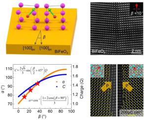
Confined low dimensional charges with high density such as two-dimensional electron gas (2DEG) at interfaces and charged domain walls in ferroelectrics show great potential to serve as functional elements in future nanoelectronics. However, stabilization and control of low dimensional charges is challenging, as they are usually subject to enormous depolarization fields. Here, we demonstrate a method to fabricate tunable charged interfaces with ~77°, 86° and 94° head-to-head polarization configurations in multiferroic BiFeO3 thin films by grain boundary engineering. The adjacent grains are cohesively bonded and the boundary is about 1 nm in width and devoid of any amorphous region. Remarkably, the polarization remains almost unchanged near the grain boundaries, indicating the polarization charges are well compensated, i.e., there should be two-dimensional charge gas confined at grain boundaries. Adjusting the tilt angle of the grain boundaries enables tuning the angle of polarization configurations from 71° to 109°, which in turn allows the control of charge density at the grain boundaries. This general and feasible method opens new doors for the application of charged interfaces in next generation nanoelectronics.
中文翻译:

具有头对头极化配置的多铁性 BiFeO3 晶界工程
具有高密度的受限低维电荷,例如界面处的二维电子气 (2DEG) 和铁电体中的带电畴壁,显示出作为未来纳米电子学中功能元件的巨大潜力。然而,低维电荷的稳定和控制具有挑战性,因为它们通常会受到巨大的去极化场的影响。在这里,我们展示了一种在多铁性 BiFeO 3中制造具有 ~77°、86° 和 94° 头对头极化配置的可调带电界面的方法晶界工程薄膜。相邻的晶粒紧密结合,边界宽度约为 1 nm,没有任何非晶区域。值得注意的是,极化在晶界附近几乎保持不变,表明极化电荷得到了很好的补偿,即在晶界处应该有二维电荷气体。调整晶界的倾斜角可以将偏振配置的角度从 71° 调整到 109°,这反过来又可以控制晶界处的电荷密度。这种通用且可行的方法为带电界面在下一代纳米电子学中的应用打开了新的大门。

















 京公网安备 11010802027423号