Our official English website, www.x-mol.net, welcomes your
feedback! (Note: you will need to create a separate account there.)
Controlled synthesis of few-layer SnSe2 by chemical vapor deposition
RSC Advances ( IF 3.9 ) Pub Date : 2020-11-19 , DOI: 10.1039/d0ra08360g
Boxing An 1, 2 , Yang Ma 1, 2 , Guoqing Zhang 1, 3 , Congya You 1, 2 , Yongzhe Zhang 1, 2
RSC Advances ( IF 3.9 ) Pub Date : 2020-11-19 , DOI: 10.1039/d0ra08360g
Boxing An 1, 2 , Yang Ma 1, 2 , Guoqing Zhang 1, 3 , Congya You 1, 2 , Yongzhe Zhang 1, 2
Affiliation
|
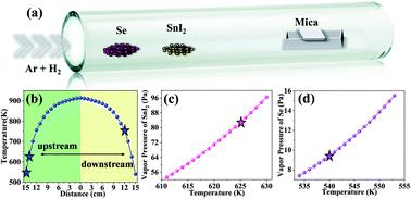
Few-layer SnSe2 has intrinsic low thermal conductivity and unique phase transition from amorphous to crystalline state under laser irradiation. It has been extensively used in the fields of thermoelectric conversion and information storage. However, the traditional precursors like tin oxide and organic compounds have either high melting points or complex compositions, and the improper deposition temperature of the substrate may lead to mixed products, which impedes controllable synthesis of high-quality few-layer SnSe2. Here, we propose a chemical vapor deposition (CVD) method, in which the precursor evaporation and deposition have been controlled via the adjustment of precursors/substrate positions, which effectively avoided mixed product growth, thus achieving the growth of high-quality few-layer SnSe2. The calculated first-order temperature coefficient of the A1g module is −0.01549 cm−1 K−1, which is superior to other two-dimensional (2D) materials. Meanwhile, two exciton emissions from few-layer SnSe2 have been found, for which the higher energy one (1.74 eV) has been assigned to near-band-gap emission, while the lower one (1.61 eV) may have roots in the surface state of SnSe2. The few-layer SnSe2 also exhibits large exciton binding energies (0.195 and 0.177 eV), which are greater than those of common semiconductors and may contribute to stability of excitons, showing broad application prospects in the field of optoelectronics.
中文翻译:

化学气相沉积法控制合成少层 SnSe2
少层SnSe 2具有固有的低热导率和在激光照射下从非晶态到晶态的独特相变。它已广泛应用于热电转换和信息存储领域。然而,传统的前驱体如氧化锡和有机化合物,要么熔点高,要么组成复杂,衬底沉积温度不当可能导致混合产物,阻碍了高质量少层SnSe 2的可控合成。在这里,我们提出了一种化学气相沉积 (CVD) 方法,其中前驱体的蒸发和沉积已经通过控制调整前驱体/衬底位置,有效避免了混合产物生长,从而实现了高质量少层SnSe 2的生长。计算得到的A 1g模块的一阶温度系数为-0.01549 cm -1 K -1,优于其他二维(2D)材料。同时,已经发现了来自少层 SnSe 2的两种激子发射,其中较高能量的一种(1.74 eV)被分配给近带隙发射,而较低的一种(1.61 eV)可能扎根于表面SnSe 2的状态。少层 SnSe 2还表现出较大的激子结合能(0.195和0.177 eV),大于普通半导体,可能有助于激子的稳定性,在光电子领域显示出广阔的应用前景。
更新日期:2020-11-19
中文翻译:
化学气相沉积法控制合成少层 SnSe2
少层SnSe 2具有固有的低热导率和在激光照射下从非晶态到晶态的独特相变。它已广泛应用于热电转换和信息存储领域。然而,传统的前驱体如氧化锡和有机化合物,要么熔点高,要么组成复杂,衬底沉积温度不当可能导致混合产物,阻碍了高质量少层SnSe 2的可控合成。在这里,我们提出了一种化学气相沉积 (CVD) 方法,其中前驱体的蒸发和沉积已经通过控制调整前驱体/衬底位置,有效避免了混合产物生长,从而实现了高质量少层SnSe 2的生长。计算得到的A 1g模块的一阶温度系数为-0.01549 cm -1 K -1,优于其他二维(2D)材料。同时,已经发现了来自少层 SnSe 2的两种激子发射,其中较高能量的一种(1.74 eV)被分配给近带隙发射,而较低的一种(1.61 eV)可能扎根于表面SnSe 2的状态。少层 SnSe 2还表现出较大的激子结合能(0.195和0.177 eV),大于普通半导体,可能有助于激子的稳定性,在光电子领域显示出广阔的应用前景。


 京公网安备 11010802027423号