当前位置:
X-MOL 学术
›
J. Phys. Chem. C
›
论文详情
Our official English website, www.x-mol.net, welcomes your
feedback! (Note: you will need to create a separate account there.)
Ga2Se3 Nanowires via Au-Assisted Heterovalent Exchange Reaction on GaAs
The Journal of Physical Chemistry C ( IF 3.3 ) Pub Date : 2020-07-20 , DOI: 10.1021/acs.jpcc.0c03216
Federico Berto 1, 2 , Niloofar Haghighian 1 , Katja Ferfolja 3 , Sandra Gardonio 3 , Mattia Fanetti 3 , Faustino Martelli 4 , Valentina Mussi 4 , Vladimir G. Dubrovskii 5 , Igor V. Shtrom 6 , Alfonso Franciosi 1, 2 , Silvia Rubini 1
Affiliation
|
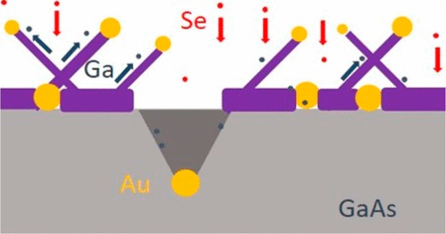
Out-of-plane Ga2Se3 nanowires are grown by molecular beam epitaxy via Au-assisted heterovalent exchange reaction on GaAs substrates in the absence of Ga deposition. It is shown that at a suitable temperature around 560 °C the Au-decorated GaAs substrate releases Ga atoms, which react with the incoming Se and feed the nanowire growth. The nanowire composition, crystal structure, and morphology are characterized by Raman spectroscopy and electron microscopy. The growth mechanism is investigated by X-ray photoelectron spectroscopy. We explore the growth parameter window and find an interesting effect of shortening of the nanowires after a certain maximum length. The nanowire growth is described within a diffusion transport model, which explains the nonmonotonic behavior of the nanowire length versus the growth parameters. Nanowire shortening is explained by the blocking of Ga supply from the GaAs substrate by thick, in-plane worm-like Ga2Se3 structures, which grow concomitantly with the nanowires, followed by backward diffusion of Ga atoms from the nanowires down to the substrate surface.
中文翻译:

Ga 2 Se 3纳米线在GaAs上的Au辅助异价交换反应
面外Ga 2 Se 3在不存在Ga沉积的情况下,通过Au辅助的异价交换反应,通过分子束外延生长纳米线。结果表明,在约560°C的合适温度下,Au装饰的GaAs衬底释放出Ga原子,该Ga原子与进入的Se反应并为纳米线的生长提供动力。通过拉曼光谱和电子显微镜表征纳米线的组成,晶体结构和形态。通过X射线光电子能谱研究了其生长机理。我们探索了生长参数窗口,并发现在一定的最大长度后缩短纳米线的有趣效果。在扩散传输模型中描述了纳米线的生长,该模型解释了纳米线长度与生长参数的非单调行为。2 Se 3结构与纳米线同时生长,然后Ga原子从纳米线向后扩散到基底表面。
更新日期:2020-08-14
中文翻译:
Ga 2 Se 3纳米线在GaAs上的Au辅助异价交换反应
面外Ga 2 Se 3在不存在Ga沉积的情况下,通过Au辅助的异价交换反应,通过分子束外延生长纳米线。结果表明,在约560°C的合适温度下,Au装饰的GaAs衬底释放出Ga原子,该Ga原子与进入的Se反应并为纳米线的生长提供动力。通过拉曼光谱和电子显微镜表征纳米线的组成,晶体结构和形态。通过X射线光电子能谱研究了其生长机理。我们探索了生长参数窗口,并发现在一定的最大长度后缩短纳米线的有趣效果。在扩散传输模型中描述了纳米线的生长,该模型解释了纳米线长度与生长参数的非单调行为。2 Se 3结构与纳米线同时生长,然后Ga原子从纳米线向后扩散到基底表面。


 京公网安备 11010802027423号