Precision Engineering ( IF 3.5 ) Pub Date : 2020-07-10 , DOI: 10.1016/j.precisioneng.2020.06.009 Liwei Ou , Sai Guo , Yan Zhe , Zhigang Dong , Renke Kang , Dongming Guo , Kang Shi
|
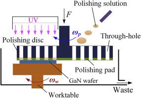
In this work, we further developed the photochemically combined mechanical polishing (PCMP) method for finishing N-type gallium nitride (GaN) wafers. A core improvement is to design a novel polishing tool with phyllotactic distributed through-holes, through which the wafer surface underneath through-holes can receive ultraviolet (UV)-light for the photochemical oxidation, while the rest parts undergo mechanical polishing. During PCMP, the co-rotation of the wafer and polishing tool allows the wafer surface to undergo the uniform and high-frequency conversion of oxidation and polishing. Based on the designed PCMP system and apparatus, the fundamental issues arising from such an alternate processing mode, which is different from the parallel mode of conventional chemical mechanical polishing (CMP), were investigated. Results show that the technical features of PCMP depend on the nature of the photochemical oxidation of wafers themselves if the mechanical polishing procedure can sufficiently remove oxides in time. The material removal rate (MRR) is inversely proportional to the dislocation density of wafers. Under acidic conditions, the oxidation proceeds by the GaN monocrystal step orientation, allowing PCMP to clear surface/subsurface damages (SSDs) and to prepare step-terrace structures on the wafer surface. When the polishing solution (pH = 1.5) includes 0.1 M K2S2O8 oxidants and 10 wt% SiO2 abrasives, the surface roughness Sa attains 0.21 nm in 10 × 10 μm2, and the MRR reaches 275.3 nm/h. The present study shows that the phyllotactic distributed through-hole array structure designed for polishing tools offers rich possibilities for the innovation of polishing technologies combining with various oxidation approaches.
中文翻译:

具有叶序分布通孔的抛光工具,用于N型氮化镓晶片的光化学联合机械抛光
在这项工作中,我们进一步开发了用于完成N型氮化镓(GaN)晶片的光化学组合机械抛光(PCMP)方法。一项核心改进是设计一种新颖的抛光工具,该抛光工具具有系统分布的通孔,通过该通孔,通孔下面的晶片表面可以接收紫外线(UV)光以进行光化学氧化,而其余部分则进行机械抛光。在PCMP期间,晶片和抛光工具的共同旋转使晶片表面经受氧化和抛光的均匀且高频的转换。基于设计的PCMP系统和设备,研究了与常规化学机械抛光(CMP)的并行模式不同的这种替代处理模式所引起的基本问题。结果表明,如果机械抛光程序能够及时地去除氧化物,则PCMP的技术特征取决于晶片本身的光化学氧化性质。材料去除率(MRR)与晶片的位错密度成反比。在酸性条件下,氧化通过GaN单晶阶梯取向进行,从而使PCMP可以清除表面/亚表面损伤(SSD)并在晶片表面上制备阶梯结构。当抛光液(pH = 1.5)包含0.1 M K 氧化通过GaN单晶阶梯取向进行,使PCMP可以清除表面/亚表面损伤(SSD),并在晶片表面上制备阶梯结构。当抛光液(pH = 1.5)包含0.1 M K 氧化通过GaN单晶阶梯取向进行,使PCMP可以清除表面/亚表面损伤(SSD),并在晶片表面上制备阶梯结构。当抛光液(pH = 1.5)包含0.1 M K2 š 2个ö 8氧化剂和10重量%的SiO 2个磨料,表面粗糙度达到萨在10×10微米的0.21纳米2,和MRR达到275.3纳米/小时。本研究表明,为抛光工具设计的叶序分布通孔阵列结构为结合各种氧化方法的抛光技术创新提供了丰富的可能性。


















 京公网安备 11010802027423号