当前位置:
X-MOL 学术
›
Adv. Mater.
›
论文详情
Our official English website, www.x-mol.net, welcomes your feedback! (Note: you will need to create a separate account there.)
Quantum Confinement of Dirac Quasiparticles in Graphene Patterned with Sub-Nanometer Precision.
Advanced Materials ( IF 27.4 ) Pub Date : 2020-06-22 , DOI: 10.1002/adma.202001119 Eva Cortés-Del Río 1 , Pierre Mallet 2, 3 , Héctor González-Herrero 1 , José Luis Lado 4 , Joaquín Fernández-Rossier 5, 6 , José María Gómez-Rodríguez 1, 7, 8 , Jean-Yves Veuillen 2, 3 , Iván Brihuega 1, 7, 8
Advanced Materials ( IF 27.4 ) Pub Date : 2020-06-22 , DOI: 10.1002/adma.202001119 Eva Cortés-Del Río 1 , Pierre Mallet 2, 3 , Héctor González-Herrero 1 , José Luis Lado 4 , Joaquín Fernández-Rossier 5, 6 , José María Gómez-Rodríguez 1, 7, 8 , Jean-Yves Veuillen 2, 3 , Iván Brihuega 1, 7, 8
Affiliation
|
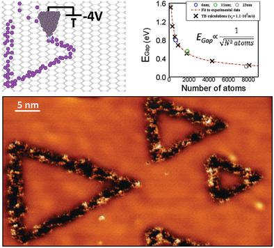
Quantum confinement of graphene Dirac‐like electrons in artificially crafted nanometer structures is a long sought goal that would provide a strategy to selectively tune the electronic properties of graphene, including bandgap opening or quantization of energy levels. However, creating confining structures with nanometer precision in shape, size, and location remains an experimental challenge, both for top‐down and bottom‐up approaches. Moreover, Klein tunneling, offering an escape route to graphene electrons, limits the efficiency of electrostatic confinement. Here, a scanning tunneling microscope (STM) is used to create graphene nanopatterns, with sub‐nanometer precision, by the collective manipulation of a large number of H atoms. Individual graphene nanostructures are built at selected locations, with predetermined orientations and shapes, and with dimensions going all the way from 2 nm up to 1 µm. The method permits the patterns to be erased and rebuilt at will, and it can be implemented on different graphene substrates. STM experiments demonstrate that such graphene nanostructures confine very efficiently graphene Dirac quasiparticles, both in 0D and 1D structures. In graphene quantum dots, perfectly defined energy bandgaps up to 0.8 eV are found that scale as the inverse of the dot’s linear dimension, as expected for massless Dirac fermions.
中文翻译:

亚纳米精度图案化石墨烯中Dirac拟粒子的量子约束。
长期以来人们一直追求在人造纳米结构中限制类石墨烯狄拉克电子的量子化,这将提供一种策略来选择性地调节石墨烯的电子性能,包括带隙开放或能级量化。但是,对于自上而下和自下而上的方法,创建形状,尺寸和位置都具有纳米精度的约束结构仍然是一项实验挑战。此外,克莱因隧穿为石墨烯电子提供了逃逸途径,从而限制了静电限制的效率。在这里,使用扫描隧道显微镜(STM)通过集体操纵大量H原子来创建亚纳米级精度的石墨烯纳米图案。在选定的位置以预定的方向和形状构建单个石墨烯纳米结构,尺寸从2 nm一直到1 µm。该方法允许随意擦除和重建图案,并且可以在不同的石墨烯基板上实施。STM实验表明,这种石墨烯纳米结构非常有效地将石墨烯Dirac准颗粒限制在0D和1D结构中。在石墨烯量子点中,发现精确定义的能带隙高达0.8 eV,与无质量的狄拉克费米子所预期的一样,该带隙与点的线性尺寸成反比。
更新日期:2020-07-28
中文翻译:
亚纳米精度图案化石墨烯中Dirac拟粒子的量子约束。
长期以来人们一直追求在人造纳米结构中限制类石墨烯狄拉克电子的量子化,这将提供一种策略来选择性地调节石墨烯的电子性能,包括带隙开放或能级量化。但是,对于自上而下和自下而上的方法,创建形状,尺寸和位置都具有纳米精度的约束结构仍然是一项实验挑战。此外,克莱因隧穿为石墨烯电子提供了逃逸途径,从而限制了静电限制的效率。在这里,使用扫描隧道显微镜(STM)通过集体操纵大量H原子来创建亚纳米级精度的石墨烯纳米图案。在选定的位置以预定的方向和形状构建单个石墨烯纳米结构,尺寸从2 nm一直到1 µm。该方法允许随意擦除和重建图案,并且可以在不同的石墨烯基板上实施。STM实验表明,这种石墨烯纳米结构非常有效地将石墨烯Dirac准颗粒限制在0D和1D结构中。在石墨烯量子点中,发现精确定义的能带隙高达0.8 eV,与无质量的狄拉克费米子所预期的一样,该带隙与点的线性尺寸成反比。


 京公网安备 11010802027423号