Our official English website, www.x-mol.net, welcomes your
feedback! (Note: you will need to create a separate account there.)
Layer-Dependent and In-Plane Anisotropic Properties of Low-Temperature Synthesized Few-Layer PdSe2 Single Crystals.
ACS Nano ( IF 15.8 ) Pub Date : 2020-04-01 , DOI: 10.1021/acsnano.0c01139
Li-Syuan Lu,Guan-Hao Chen,Hui-Yu Cheng,Chih-Piao Chuu,Kuan-Cheng Lu,Chia-Hao Chen,Ming-Yen Lu,Tzu-Hung Chuang,Der-Hsin Wei,Wei-Chen Chueh,Wen-Bin Jian,Ming-Yang Li,Yu-Ming Chang,Lain-Jong Li,Wen-Hao Chang
ACS Nano ( IF 15.8 ) Pub Date : 2020-04-01 , DOI: 10.1021/acsnano.0c01139
Li-Syuan Lu,Guan-Hao Chen,Hui-Yu Cheng,Chih-Piao Chuu,Kuan-Cheng Lu,Chia-Hao Chen,Ming-Yen Lu,Tzu-Hung Chuang,Der-Hsin Wei,Wei-Chen Chueh,Wen-Bin Jian,Ming-Yang Li,Yu-Ming Chang,Lain-Jong Li,Wen-Hao Chang
|
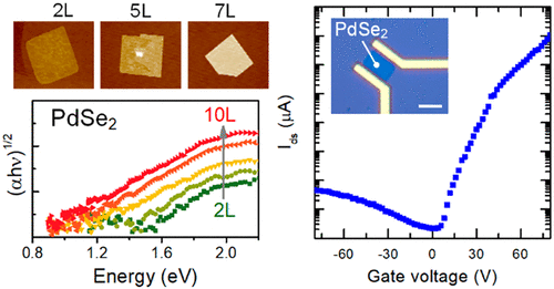
Palladium diselenide (PdSe2), a peculiar noble metal dichalcogenide, has emerged as a new two-dimensional material with high predicted carrier mobility and a widely tunable band gap for device applications. The inherent in-plane anisotropy endowed by the pentagonal structure further renders PdSe2 promising for novel electronic, photonic, and thermoelectric applications. However, the direct synthesis of few-layer PdSe2 is still challenging and rarely reported. Here, we demonstrate that few-layer, single-crystal PdSe2 flakes can be synthesized at a relatively low growth temperature (300 °C) on sapphire substrates using low-pressure chemical vapor deposition (CVD). The well-defined rectangular domain shape and precisely determined layer number of the CVD-grown PdSe2 enable us to investigate their layer-dependent and in-plane anisotropic properties. The experimentally determined layer-dependent band gap shrinkage combined with first-principle calculations suggest that the interlayer interaction is weaker in few-layer PdSe2 in comparison with that in bulk crystals. Field-effect transistors based on the CVD-grown PdSe2 also show performances comparable to those based on exfoliated samples. The low-temperature synthesis method reported here provides a feasible approach to fabricate high-quality few-layer PdSe2 for device applications.
中文翻译:

低温合成的几层PdSe2单晶的层相关和面内各向异性特性。
二硒化钯(PdSe2)是一种特殊的贵金属二卤化钴,已成为一种新型的二维材料,具有很高的预计载流子迁移率和可广泛调节的带隙,可用于设备应用。五边形结构赋予的固有平面内各向异性进一步使PdSe2有望用于新型电子,光子和热电应用。然而,几层PdSe2的直接合成仍然具有挑战性,很少报道。在这里,我们证明了使用低压化学气相沉积(CVD)可以在相对较低的生长温度(300°C)下在蓝宝石衬底上合成几层单晶PdSe2薄片。CVD生长的PdSe2的定义明确的矩形畴形状和精确确定的层数使我们能够研究它们的层依赖性和面内各向异性特性。实验确定的与层有关的带隙收缩率与第一性原理的结合表明,与块状晶体相比,几层PdSe2中的层间相互作用较弱。基于CVD生长的PdSe2的场效应晶体管也显示出与基于剥离样品的场效应晶体管相当的性能。本文报道的低温合成方法提供了一种可行的方法来制造用于器件应用的高质量多层PdSe2。
更新日期:2020-04-01
中文翻译:
低温合成的几层PdSe2单晶的层相关和面内各向异性特性。
二硒化钯(PdSe2)是一种特殊的贵金属二卤化钴,已成为一种新型的二维材料,具有很高的预计载流子迁移率和可广泛调节的带隙,可用于设备应用。五边形结构赋予的固有平面内各向异性进一步使PdSe2有望用于新型电子,光子和热电应用。然而,几层PdSe2的直接合成仍然具有挑战性,很少报道。在这里,我们证明了使用低压化学气相沉积(CVD)可以在相对较低的生长温度(300°C)下在蓝宝石衬底上合成几层单晶PdSe2薄片。CVD生长的PdSe2的定义明确的矩形畴形状和精确确定的层数使我们能够研究它们的层依赖性和面内各向异性特性。实验确定的与层有关的带隙收缩率与第一性原理的结合表明,与块状晶体相比,几层PdSe2中的层间相互作用较弱。基于CVD生长的PdSe2的场效应晶体管也显示出与基于剥离样品的场效应晶体管相当的性能。本文报道的低温合成方法提供了一种可行的方法来制造用于器件应用的高质量多层PdSe2。


 京公网安备 11010802027423号