Nature Communications ( IF 14.7 ) Pub Date : 2020-03-23 , DOI: 10.1038/s41467-020-15181-4 Min Je Kim , Myeongjae Lee , Honggi Min , Seunghan Kim , Jeehye Yang , Hyukmin Kweon , Wooseop Lee , Do Hwan Kim , Jong-Ho Choi , Du Yeol Ryu , Moon Sung Kang , BongSoo Kim , Jeong Ho Cho
|
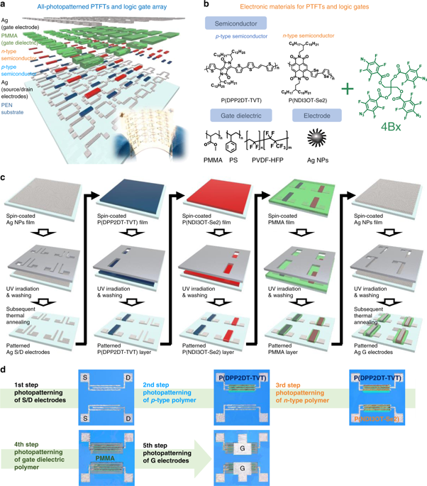
All-solution processing of large-area organic electronics requires multiple steps of patterning and stacking of various device components. Here, we report the fabrication of highly integrated arrays of polymer thin-film transistors and logic gates entirely through a series of solution processes. The fabrication is done using a three-dimensional crosslinker in tetrahedral geometry containing four photocrosslinkable azide moieties, referred to as 4Bx. 4Bx can be mixed with a variety of solution-processable electronic materials (polymer semiconductors, polymer insulators, and metal nanoparticles) and generate crosslinked network under exposure to UV. Fully crosslinked network film can be formed even at an unprecedentedly small loading, which enables preserving the inherent electrical and structural characteristics of host material. Because the crosslinked electronic component layers are strongly resistant to chemical solvents, micropatterning the layers at high resolution as well as stacking the layers on top of each other by series of solution processing steps is possible.
中文翻译:

适用于全光图案电子产品的通用三维交联剂
大面积有机电子产品的全解决方案处理需要对各种设备组件进行构图和堆叠的多个步骤。在这里,我们报告完全通过一系列解决方案制造的聚合物薄膜晶体管和逻辑门的高度集成阵列。使用四面体几何形状的三维交联剂完成制造,该交联剂包含四个可光交联的叠氮化物部分,称为4Bx。4Bx可以与多种可溶液处理的电子材料(聚合物半导体,聚合物绝缘体和金属纳米颗粒)混合,并在暴露于紫外线下产生交联网络。甚至可以以前所未有的小负载形成完全交联的网络薄膜,这可以保留基质材料的固有电学和结构特征。














 京公网安备 11010802027423号