当前位置:
X-MOL 学术
›
Adv. Mater.
›
论文详情
Our official English website, www.x-mol.net, welcomes your
feedback! (Note: you will need to create a separate account there.)
Controllable Growth of High-Quality Inorganic Perovskite Microplate Arrays for Functional Optoelectronics.
Advanced Materials ( IF 27.4 ) Pub Date : 2020-03-12 , DOI: 10.1002/adma.201908006
Zhenkun Gu 1, 2 , Zhonghao Zhou 1, 2 , Zhandong Huang 1, 2 , Kang Wang 1, 2 , Zheren Cai 1, 2 , Xiaotian Hu 1, 2 , Lihong Li 1 , Mingzhu Li 1 , Yong Sheng Zhao 1 , Yanlin Song 1
Advanced Materials ( IF 27.4 ) Pub Date : 2020-03-12 , DOI: 10.1002/adma.201908006
Zhenkun Gu 1, 2 , Zhonghao Zhou 1, 2 , Zhandong Huang 1, 2 , Kang Wang 1, 2 , Zheren Cai 1, 2 , Xiaotian Hu 1, 2 , Lihong Li 1 , Mingzhu Li 1 , Yong Sheng Zhao 1 , Yanlin Song 1
Affiliation
|
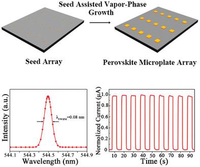
Inorganic perovskite single crystals have emerged as promising vapor-phase processable structures for optoelectronic devices. However, because of material lattice mismatch and uncontrolled nucleation, vapor-phase methods have been restricted to random distribution of single crystals that are difficult to perform for integrated device arrays. Herein, an effective strategy to control the vapor-phase growth of high-quality cesium lead bromide perovskite (CsPbBr3 ) microplate arrays with uniform morphology as well as controlled location and size is reported. By introducing perovskite seeds on substrates, intractable lattice mismatches and random nucleation barriers are surpassed, and the epitaxial growth of perovskite crystals is accurately controlled. It is further demonstrated that CsPbBr3 microplate arrays can be monolithically integrated on substrates for the fabrication of high-performance lasers and photodetectors. This strategy provides a facile approach to fabricate high-quality CsPbBr3 microplates with controllable size and location, which offers new opportunities for the scalable production of integrated optoelectronic devices.
中文翻译:

用于功能光电的高质量无机钙钛矿微孔板阵列的可控生长。
无机钙钛矿单晶已成为光电子器件的有希望的气相可加工结构。但是,由于材料晶格失配和不受控制的成核作用,气相方法已被限制为单晶的随机分布,这对于集成器件阵列而言很难执行。在本文中,报告了一种有效的策略来控制具有均匀形态以及受控位置和大小的高质量溴化钙铯铅钙钛矿(CsPbBr3)微孔板阵列的气相生长。通过在衬底上引入钙钛矿种子,可以克服顽固的晶格失配和无规成核障碍,并且可以精确地控制钙钛矿晶体的外延生长。进一步证明,CsPbBr3微孔板阵列可以单片集成在基板上,用于制造高性能激光器和光电探测器。该策略为制造尺寸和位置可控的高质量CsPbBr3微孔板提供了一种简便的方法,这为可扩展生产集成光电器件提供了新的机遇。
更新日期:2020-04-21
中文翻译:
用于功能光电的高质量无机钙钛矿微孔板阵列的可控生长。
无机钙钛矿单晶已成为光电子器件的有希望的气相可加工结构。但是,由于材料晶格失配和不受控制的成核作用,气相方法已被限制为单晶的随机分布,这对于集成器件阵列而言很难执行。在本文中,报告了一种有效的策略来控制具有均匀形态以及受控位置和大小的高质量溴化钙铯铅钙钛矿(CsPbBr3)微孔板阵列的气相生长。通过在衬底上引入钙钛矿种子,可以克服顽固的晶格失配和无规成核障碍,并且可以精确地控制钙钛矿晶体的外延生长。进一步证明,CsPbBr3微孔板阵列可以单片集成在基板上,用于制造高性能激光器和光电探测器。该策略为制造尺寸和位置可控的高质量CsPbBr3微孔板提供了一种简便的方法,这为可扩展生产集成光电器件提供了新的机遇。


 京公网安备 11010802027423号