当前位置:
X-MOL 学术
›
Adv. Funct. Mater.
›
论文详情
Our official English website, www.x-mol.net, welcomes your
feedback! (Note: you will need to create a separate account there.)
High‐Speed Organic Single‐Crystal Transistor Responding to Very High Frequency Band
Advanced Functional Materials ( IF 18.5 ) Pub Date : 2020-02-05 , DOI: 10.1002/adfm.201909501 Akifumi Yamamura 1, 2 , Takaaki Sakon 1 , Kayo Takahira 1 , Takahiro Wakimoto 1, 3 , Mari Sasaki 1 , Toshihiro Okamoto 1, 2, 4 , Shun Watanabe 1, 2, 4 , Jun Takeya 1, 2, 3, 5
Advanced Functional Materials ( IF 18.5 ) Pub Date : 2020-02-05 , DOI: 10.1002/adfm.201909501 Akifumi Yamamura 1, 2 , Takaaki Sakon 1 , Kayo Takahira 1 , Takahiro Wakimoto 1, 3 , Mari Sasaki 1 , Toshihiro Okamoto 1, 2, 4 , Shun Watanabe 1, 2, 4 , Jun Takeya 1, 2, 3, 5
Affiliation
|
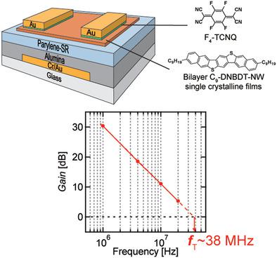
Although high carrier mobility organic field‐effect transistors (OFETs) are required for high‐speed device applications, improving the carrier mobility alone does not lead to high‐speed operation. Because the cut‐off frequency is determined predominantly by the total resistance and parasitic capacitance of a transistor, it is necessary to miniaturize OFETs while reducing these factors. Depositing a dopant layer only at the metal/semiconductor interface is an effective technique to reduce the contact resistance. However, fine‐patterning techniques for a dopant layer are still challenging especially for a top‐contact solution‐processed OFET geometry because organic semiconductors are vulnerable to chemical damage by solvents. In this work, high‐resolution, damage‐free patterning of a dopant layer is developed to fabricate short‐channel OFETs with a dopant interlayer inserted at the contacts. The fabricated OFETs exhibit high mobility exceeding 10 cm2 V−1 s−1 together with a reasonably low contact resistance, allowing for high frequency operation at 38 MHz. In addition, a diode‐connected OFET shows a rectifying capability of up to 78 MHz at an applied voltage of 5 V. This shows that an OFET can respond to the very high frequency band, which is beneficial for long‐distance wireless communication.
中文翻译:

响应极高频段的高速有机单晶晶体管
尽管高速设备应用需要高载流子迁移率有机场效应晶体管(OFET),但仅提高载流子迁移率并不能带来高速运行。由于截止频率主要由晶体管的总电阻和寄生电容决定,因此有必要在减小这些因素的同时使OFET小型化。仅在金属/半导体界面处沉积掺杂剂层是降低接触电阻的有效技术。但是,由于有机半导体很容易受到溶剂的化学破坏,因此对于掺杂剂层的精细构图技术仍然具有挑战性,尤其是对于顶部接触溶液加工的OFET几何形状。在这项工作中,高分辨率 掺杂剂层的无损伤图案被开发出来以制造短通道的OFET,其在触点处插入了掺杂剂中间层。制成的OFET具有超过10厘米的高迁移率2 V -1 s -1以及相当低的接触电阻,允许在38 MHz下进行高频工作。此外,二极管连接的OFET在施加5 V电压时显示出高达78 MHz的整流能力。这表明,OFET可以响应非常高的频带,这对于长距离无线通信是有益的。
更新日期:2020-03-10
中文翻译:
响应极高频段的高速有机单晶晶体管
尽管高速设备应用需要高载流子迁移率有机场效应晶体管(OFET),但仅提高载流子迁移率并不能带来高速运行。由于截止频率主要由晶体管的总电阻和寄生电容决定,因此有必要在减小这些因素的同时使OFET小型化。仅在金属/半导体界面处沉积掺杂剂层是降低接触电阻的有效技术。但是,由于有机半导体很容易受到溶剂的化学破坏,因此对于掺杂剂层的精细构图技术仍然具有挑战性,尤其是对于顶部接触溶液加工的OFET几何形状。在这项工作中,高分辨率 掺杂剂层的无损伤图案被开发出来以制造短通道的OFET,其在触点处插入了掺杂剂中间层。制成的OFET具有超过10厘米的高迁移率2 V -1 s -1以及相当低的接触电阻,允许在38 MHz下进行高频工作。此外,二极管连接的OFET在施加5 V电压时显示出高达78 MHz的整流能力。这表明,OFET可以响应非常高的频带,这对于长距离无线通信是有益的。


 京公网安备 11010802027423号